Step-up circuit

A booster circuit and circuit technology, which is applied in the direction of electrical components, static memory, instruments, etc., can solve the problems of transistor characteristic degradation and influence, and achieve the effect of suppressing characteristic degradation

Inactive Publication Date: 2014-11-05
PANASONIC INTELLECTUAL PROPERTY MANAGEMENT CO LTD
View PDF11 Cites 4 Cited by
  • Summary
  • Abstract
  • Description
  • Claims
  • Application Information

AI Technical Summary

Problems solved by technology

In particular, the upper limit of the boosted voltage affects the deterioration of the characteristics of transistors supplied with the boosted voltage

Method used


Image

  • Step-up circuit
  • Step-up circuit
  • Step-up circuit

Examples


Embodiment Construction

[0031] Hereinafter, embodiments of the present invention will be described with reference to the drawings.

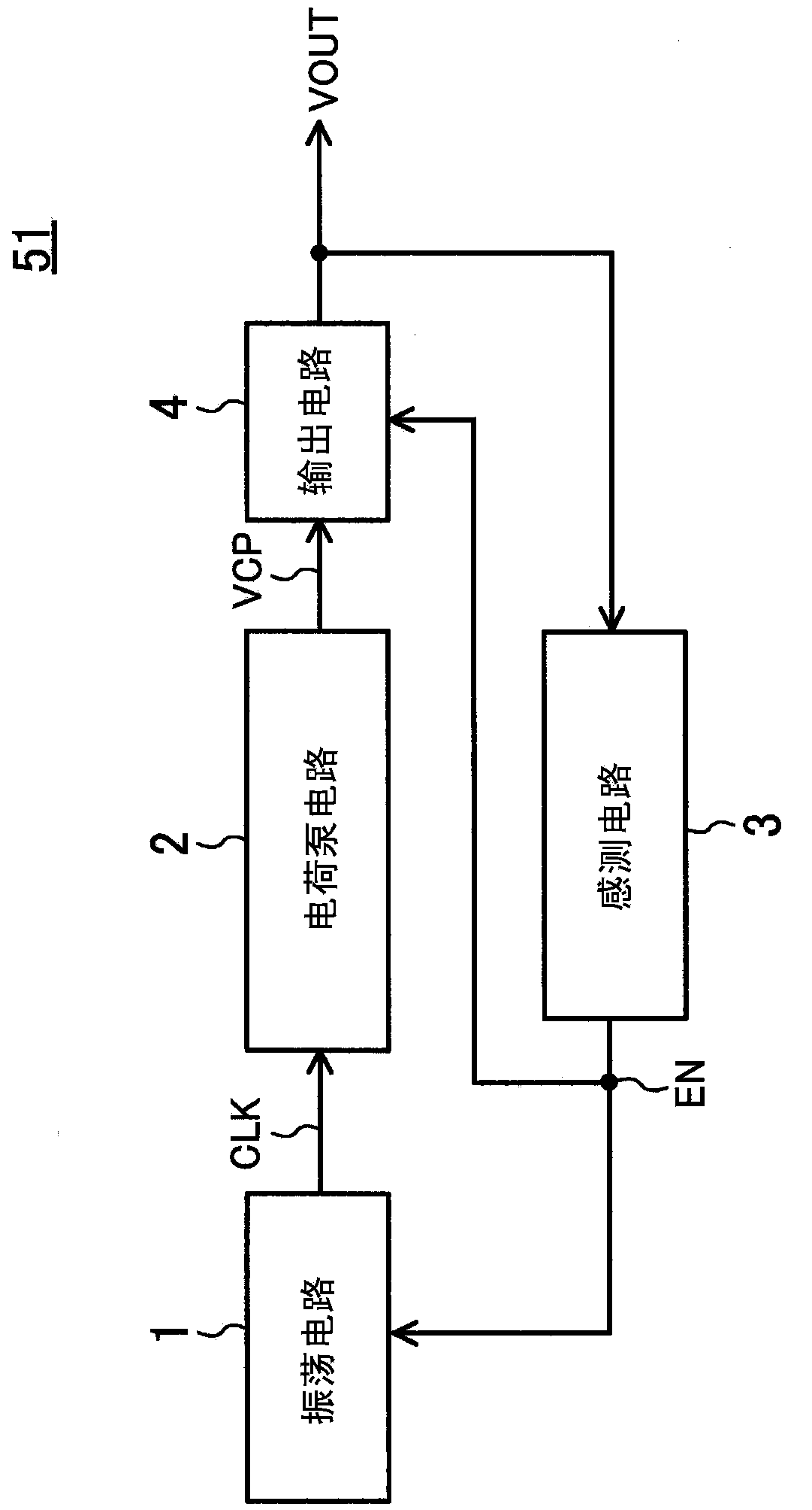
[0032] figure 1 The configuration of the booster circuit 51 according to the embodiment of the present invention is shown. figure 1 The boost circuit 51 is a circuit that boosts the supply voltage to obtain the output VOUT of the boost circuit, and includes: an oscillation circuit 1 that generates a clock signal CLK; boosts the supply voltage using the clock signal CLK, thereby obtaining the charge pump output VCP The charge pump circuit 2; the sensing circuit 3 that senses the voltage of the boost circuit output VOUT and outputs the sensing signal EN; and the output circuit 4 that cuts off the connection between the charge pump output VCP and the boost circuit output VOUT. The sensing circuit 3 outputs a sensing signal EN according to the output VOUT of the booster circuit.

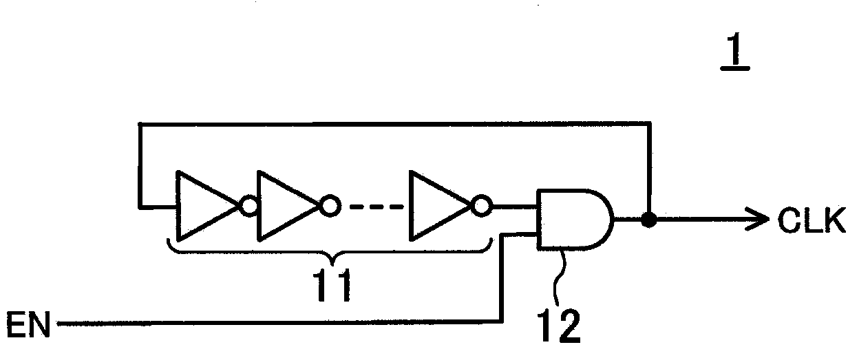
[0033] figure 2 express figure 1 An example of the oscillator circuit 1 in figure 2 The...


PUM


Abstract

A booster circuit configured to boost a supplied voltage and provide a booster circuit output includes: an oscillator circuit configured to generate a clock signal; a charge pump circuit configured to provide a charge pump output by boosting the supplied voltage with the use of the clock signal; a detection circuit configured to detect a voltage of the booster circuit output and output a detection signal; and an output circuit configured to connect and disconnect the charge pump output to and from the booster circuit output. The oscillator circuit controls activation and deactivation of an output of the oscillator circuit in accordance with the detection signal, and the output circuit controls disconnection of the output circuit in accordance with the detection signal.

Description

technical field [0001] The present invention relates to a boost circuit used in semiconductor memories, and more particularly to a boost circuit that reduces overshoot and ripple of the boost voltage. Background technique [0002] A semiconductor memory such as a flash memory requires a higher voltage than an external power supply voltage in order to perform data writing, erasing, and reading operations. Such a semiconductor memory has a booster circuit that includes: an oscillation circuit that generates a clock signal, a charge pump circuit that boosts a supply voltage using the clock signal, and senses the boosted voltage and maintains the boosted voltage at a certain level. The sensing circuit is controlled by means of a voltage range. [0003] The voltage range of the boosted voltage affects the stable operation of the circuit supplied with the boosted voltage. In particular, the upper limit of the boosted voltage affects the deterioration of the characteristics of tr...

Claims


Application Information

Patent Timeline
Patent Type & Authority Applications(China)
IPC IPC(8): H02M3/07G11C5/14G11C16/06
CPCH02M3/07G11C5/145G11C13/0021G11C7/12H02M3/073G11C11/165G11C16/12G11C8/08
Inventor 滨本幸昌
Owner PANASONIC INTELLECTUAL PROPERTY MANAGEMENT CO LTD
Why Eureka
Try Eureka