Semiconductor detection circuit and method

A detection circuit and detection method technology, applied in the direction of testing circuits, semiconductor devices, circuits, etc., can solve the problems of long detection time and high detection cost, and achieve the effect of saving detection time and cost

Active Publication Date: 2014-11-12
SEMICON MFG INT (SHANGHAI) CORP
View PDF12 Cites 3 Cited by
  • Summary
  • Abstract
  • Description
  • Claims
  • Application Information

AI Technical Summary

Problems solved by technology

[0003] In order to obtain a metal interconnect structure with better breakdown characteristics, it is usually necessary to detect multiple groups of metal interconnect structures with different metal interconnect line spacing, shape or different dielectric materials. If the existing detection method is used, only one gro

Method used


Image

  • Semiconductor detection circuit and method
  • Semiconductor detection circuit and method
  • Semiconductor detection circuit and method

Examples


Embodiment Construction

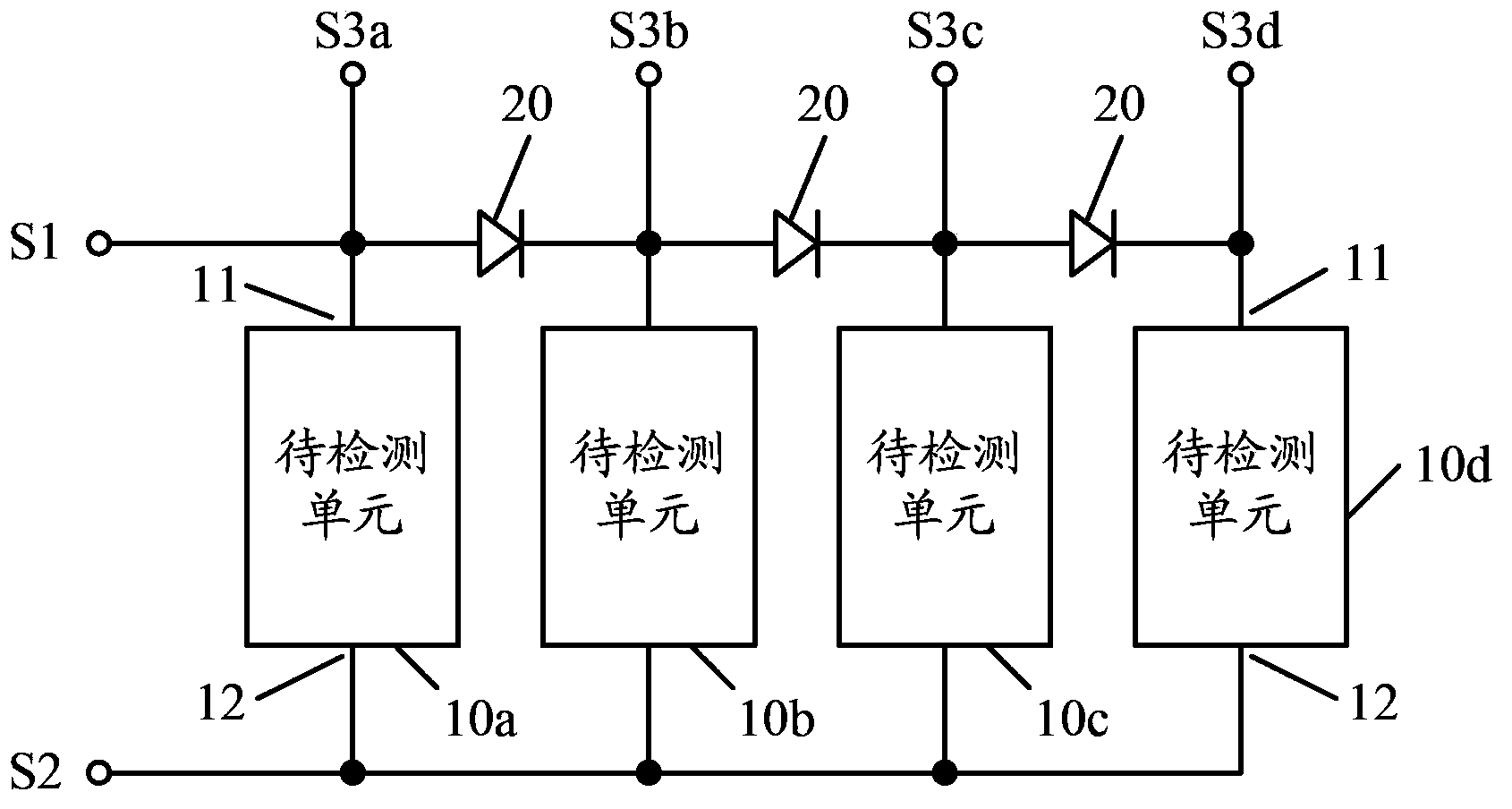
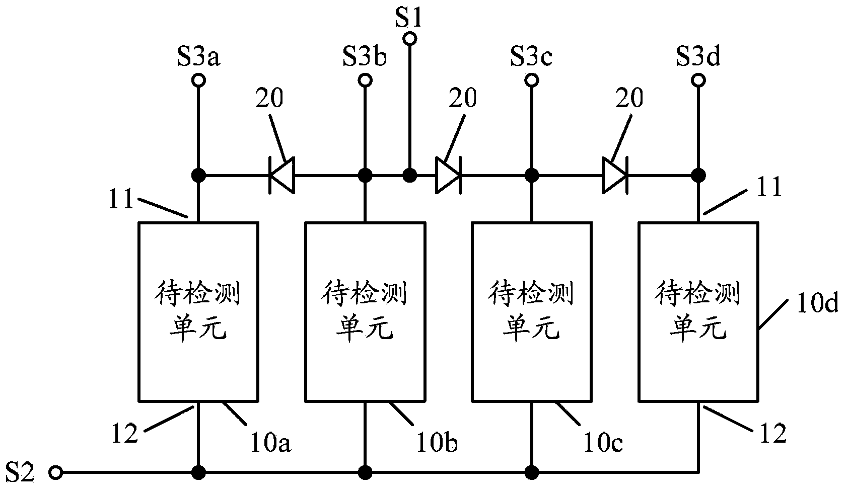
[0026] Since the detection time of detection by existing detection methods is relatively long, the present invention provides a semiconductor detection circuit and a detection method. First, a breakdown detection voltage is applied to the first detection end of the semiconductor detection circuit, and the second detection end Grounded, the third detection terminal floating, until at least one of the units to be detected is broken down, a current is detected between the first detection terminal and the second detection terminal, and the application of the breakdown detection voltage is stopped; A detection voltage is applied to the detection terminals, the first detection terminal is floating, and the third detection terminal is grounded. When at least one of the third detection terminals detects a current, it indicates that the corresponding unit to be detected is first broken down. Since the structure of each unit to be detected is different, by knowing the unit to be detected...


PUM


Abstract

The invention provides a semiconductor detection circuit and method. The semiconductor detection circuit comprises at least two parallel units to be detected, a first detection end, a second detection end, at least two third detection ends corresponding to the units to be detected one to one and at least one diode. The units to be detected are used for detecting breakdown characteristics between two electrodes, and the structures of the different units to be detected are different. The second ends of every two adjacent units to be detected are connected with the second detection end, the first ends of every two adjacent units to be detected are connected through the diodes, the first end of one unit to be detected is connected with the first detection end, the anodes of all the diodes face the first detection end, and therefore all the diodes are switched on when the first detection end applies forward breakdown detection voltages. By the adoption of the semiconductor detection circuit, the unit to be detected with the worst voltage withstanding characteristic can be quickly detected, and different influences of the structures of the different units to be detected on the breakdown characteristics can be acquired.

Description

technical field [0001] The invention relates to semiconductor detection technology, in particular to a semiconductor detection circuit and a detection method. Background technique [0002] In the existing semiconductor technology, a multilayer metal interconnection structure is usually used to electrically connect various devices, and the metal interconnections are electrically isolated by dielectric materials with good insulating properties. The reliability of the multilayer metal interconnection structure is crucial to the yield, product performance and reliability of the entire IC manufacturing process. Therefore, the breakdown and The reliability test of the time-dependent dielectric breakdown (Time dependent Dielectric Breakdown, TDDB) characteristic has become an extremely important test item in the reliability test. In the reliability test, by applying a voltage to the adjacent metal interconnection lines, electric leakage occurs between the adjacent metal interconne...

Claims


Application Information

Patent Timeline
IPC IPC(8): G01R31/14H01L23/544
Inventor 冯军宏周洁
Owner SEMICON MFG INT (SHANGHAI) CORP
Why Eureka
Try Eureka