
Epitaxial wafer of LED (Light Emitting Diode) and manufacturing method thereof

A technology of light-emitting diodes and a manufacturing method, which is applied in the directions of electrical components, circuits, semiconductor devices, etc., to achieve the effect of improving the recombination efficiency

Inactive Publication Date: 2014-11-19
XIANGNENG HUALEI OPTOELECTRONICS
View PDF6 Cites 2 Cited by
  • Summary
  • Abstract
  • Description
  • Claims
  • Application Information

AI Technical Summary

Problems solved by technology

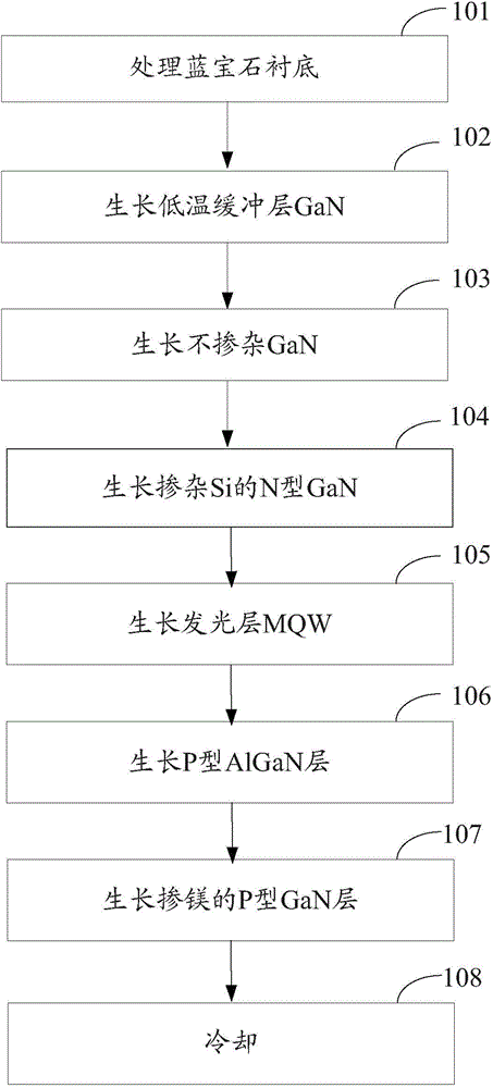
Using the traditional LED MOCVD epitaxial growth technology to grow the light-emitting layer of the epitaxial wafer generally needs to grow 14-16 cycles (the so-called cycle is the number of times to repeat the growth of a unit, a unit consists of two materials, and periodic growth means not doing any Changed repeated growth unit material), while the hole filling period is 5-6 positions close to the P layer, and the electrons are filled in the 14-16 period, and the filling concentration of electrons from the N layer to the P layer is decreasing, close to The period number of the N layer reaches 9-10 and does not participate in light emission (the 9-10 period unit material near the N layer does not emit light because there are no holes, and the material does not participate in light emission), because the hole concentration (the concentration of the hole It is not the electron concentration, the hole is a physical definition particle opposite to the electron, please refer to semiconductor physics) is almost zero, and the recombination efficiency is almost zero

Method used


Image

  • Epitaxial wafer of LED (Light Emitting Diode) and manufacturing method thereof
  • Epitaxial wafer of LED (Light Emitting Diode) and manufacturing method thereof
  • Epitaxial wafer of LED (Light Emitting Diode) and manufacturing method thereof

Examples


Embodiment Construction

[0037] Certain terms are used, for example, in the description and claims to refer to particular components. Those skilled in the art should understand that hardware manufacturers may use different terms to refer to the same component. The specification and claims do not use the difference in name as a way to distinguish components, but use the difference in function of components as a criterion for distinguishing. As mentioned throughout the specification and claims, "comprising" is an open term, so it should be interpreted as "including but not limited to". "Approximately" means that within an acceptable error range, those skilled in the art can solve the technical problem within a certain error range and basically achieve the technical effect. The subsequent description of the specification is a preferred implementation mode for implementing the application, but the description is for the purpose of illustrating the general principle of the application, and is not intended...


PUM


Abstract

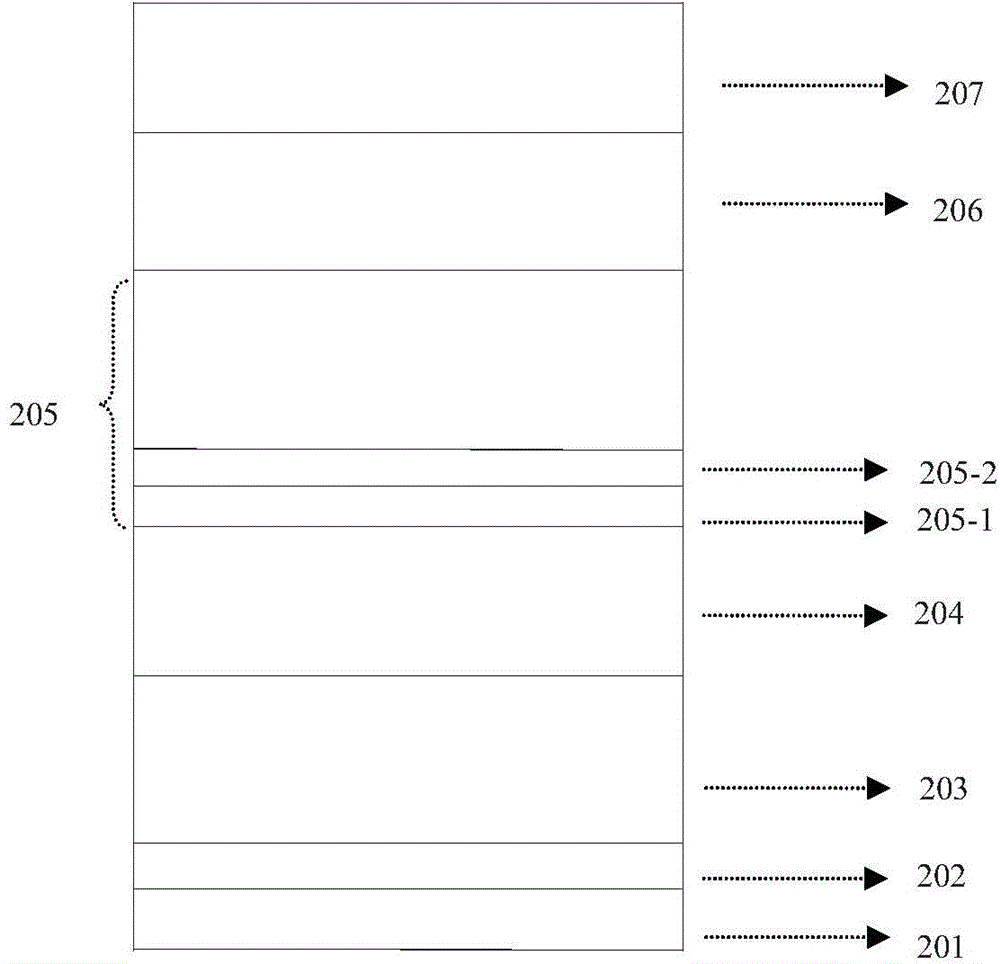
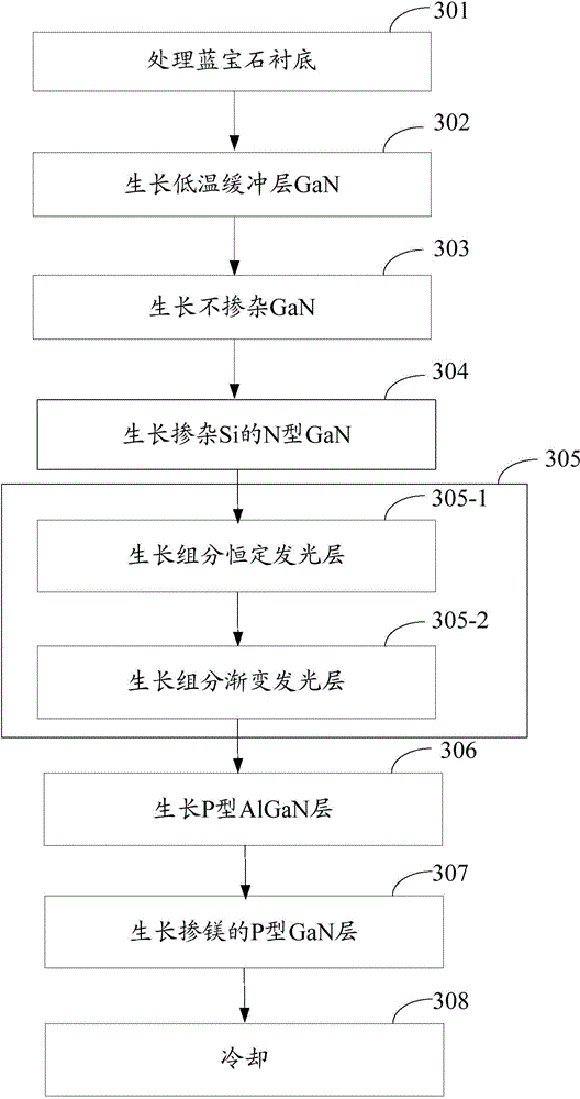
The application discloses an epitaxial wafer of an LED (Light Emitting Diode) and a manufacturing method thereof. The epitaxial wafer of the LED comprises an Si-doped GaN layer, a component constant luminous layer positioned above the Si-doped GaN layer, a component gradually-changed luminous layer positioned above the component constant luminous layer, and a P-type AlGaN layer positioned above the component gradually-changed luminous layer, wherein the component gradually-changed luminous layer comprises a GaN layer and an In-doped InGaN layer; the doped In concentrations of InGaN layers in all the cycles are different. Compared with the prior art, the epitaxial wafer disclosed by the application can adjust the distribution of the luminous layer in the electron filling state, and the energy band of the luminous layer is adjusted, so that the hole and electron compositing efficiency is improved.

Description

technical field [0001] The present application relates to the manufacturing technology of light-emitting diode chips, and more specifically, to an epitaxial wafer with a graded energy band and a manufacturing method thereof. Background technique [0002] A light-emitting diode (Light-Emitting Diode, referred to as LED) is a semiconductor electronic device that converts electrical energy into light energy. When electric current flows, electrons and holes recombine in it to emit monochromatic light. LED lighting has been widely used in home, decoration, office, signboard and even street lighting. The chip structure design of LDE is a very complex system engineering, which involves the design of the electroluminescent structure for the purpose of improving the injection efficiency and light efficiency, the design of the light extraction structure for the purpose of improving the light extraction efficiency, and the light-efficiency-related issues. electrode design, etc. [0...

Claims


Application Information

Patent Timeline
IPC IPC(8): H01L33/06H01L33/00
CPCH01L33/06H01L33/08H01L33/32H01L33/325
Inventor 马海庆张宇徐迪
Owner XIANGNENG HUALEI OPTOELECTRONICS
Learn More