Light-emitting diode with composite polar face electron blocking layer

An electron blocking layer, light-emitting diode technology, applied in circuits, electrical components, semiconductor devices, etc., can solve the problems of large lattice mismatch, uneven distribution of carriers, low carrier recombination efficiency and low luminous efficiency, etc. Achieve the effect of increasing the probability and reducing the leakage current

Active Publication Date: 2016-08-17
SOUTHEAST UNIV
View PDF7 Cites 15 Cited by
  • Summary
  • Abstract
  • Description
  • Claims
  • Application Information

AI Technical Summary

Problems solved by technology

Although these electron blocking layers have many advantages, they still cannot satisfactorily solve the following technical problems: 1) the more obvious the effect of the p-type electron blocking layer on electron blocking, the greater the drop in hole injection efficiency; The lattice mismatch between the

Method used


Image

  • Light-emitting diode with composite polar face electron blocking layer
  • Light-emitting diode with composite polar face electron blocking layer
  • Light-emitting diode with composite polar face electron blocking layer

Examples


Example Embodiment

[0033] Example

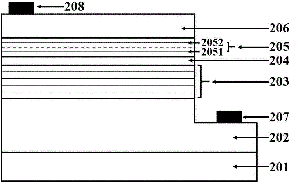
[0034] Such as figure 2 Shown is an LED with a composite polarity surface electron blocking layer, including a sapphire substrate 201, a metal polarity surface n-type GaN layer 202, a metal polarity surface InGaN / GaN multiple quantum well layer 203, which are sequentially arranged from bottom to top. The metal polar plane p-type AlGaN layer 204 is composed of a metal polar plane p-type electron barrier layer 2051 of a GaN / AlGaN superlattice structure and a nitrogen polar plane p-type electron barrier layer 2052 of a GaN / AlGaN superlattice structure A composite polar plane p-type electron blocking layer 205, a nitrogen polar plane p-type GaN layer 206, an n electrode 207 arranged on the metal polar plane n-type GaN layer, and a nitrogen polar plane p-type GaN layer 的p-electrode 208.

[0035] The metal-polar plane n-type GaN layer 202 is used as the n-type region of the LED, and its thickness is between 0.5 and 2 μm. The layer is doped with Si element, and the free...


PUM

PropertyMeasurementUnit
Thicknessaaaaaaaaaa
Thicknessaaaaaaaaaa
Thicknessaaaaaaaaaa

Abstract

The invention discloses a light-emitting diode with a composite polar face electron blocking layer. The light-emitting diode comprises a substrate (101), a metal polar face n-type nitride layer (102), a metal polar face multiple quantum well layer (103), a metal polar face p-type nitride layer (104), a composite polar face p-type electron blocking layer (105) composed of a metal polar face p-type electron blocking layer (1051) and a nitrogen polar face p-type electron blocking layer (1052), a nitrogen polar face p-type nitride layer (106), an n electrode (7) arranged on the metal polar face n-type nitride layer and a p electrode (8) arranged on the nitrogen polar face p-type nitride layer, and the layers and the electrodes are arranged sequentially from bottom to top. A high electronic barrier is formed on a conduction band by the composite polar face electron blocking layer and blocks electrons from crossing a multiple quantum well active region to enter a p-type region, leakage currents can be reduced, and the probability of radiative recombination of the electrons and holes is improved.

Description

technical field [0001] The invention provides a light-emitting diode (LED) with a composite polar surface electron blocking layer, which belongs to the field of manufacturing semiconductor optoelectronic materials and devices. Background technique [0002] LED has attracted much attention due to its advantages of high efficiency, energy saving, small size, and long life, and has begun to gradually replace traditional lighting methods such as fluorescent lamps and incandescent lamps. However, the rapid decline of the internal quantum efficiency of LEDs under the condition of high current injection seriously restricts the application and development of LEDs, and the leakage current is considered to be a main factor leading to the decline of LED efficiency under the condition of high current density. Therefore, reducing the leakage current is very important for improving the luminous efficiency of the LED. [0003] Since electrons have a smaller effective mass and higher mobil...

Claims


Application Information

Patent Timeline
IPC IPC(8): H01L33/14H01L33/06H01L33/12H01L33/32
CPCH01L33/06H01L33/12H01L33/145H01L33/32
Inventor 张雄王南崔一平
Owner SOUTHEAST UNIV
Why Eureka
Try Eureka