Epitaxial wafer of light emitting diode and preparation method thereof

A technology of light-emitting diodes and epitaxial wafers, applied in the direction of electrical components, circuits, semiconductor devices, etc., can solve the problems of low luminous efficiency and low recombination efficiency of light-emitting diodes, and achieve the effects of strengthening the limiting effect, improving recombination efficiency, and improving luminous efficiency

Inactive Publication Date: 2019-02-19
HC SEMITEK ZHEJIANG CO LTD
View PDF5 Cites 17 Cited by
  • Summary
  • Abstract
  • Description
  • Claims
  • Application Information

AI Technical Summary

Problems solved by technology

However, based on the physical characteristics of the holes themselves, the number of holes that can be formed in the P-type GaN layer is small, resulting in holes that can enter the InGaN / GaN multi-quantum well layer and emit light with electrons in the InGaN / GaN multi-quantum well layer. The number of holes is limited, the recombination efficiency of a large number of electrons from the N-type GaN layer in the InGaN / GaN multi-quantum well layer is low, and the luminous efficiency of the light-emitting diode is low

Method used


Image

  • Epitaxial wafer of light emitting diode and preparation method thereof
  • Epitaxial wafer of light emitting diode and preparation method thereof
  • Epitaxial wafer of light emitting diode and preparation method thereof

Examples


Embodiment Construction

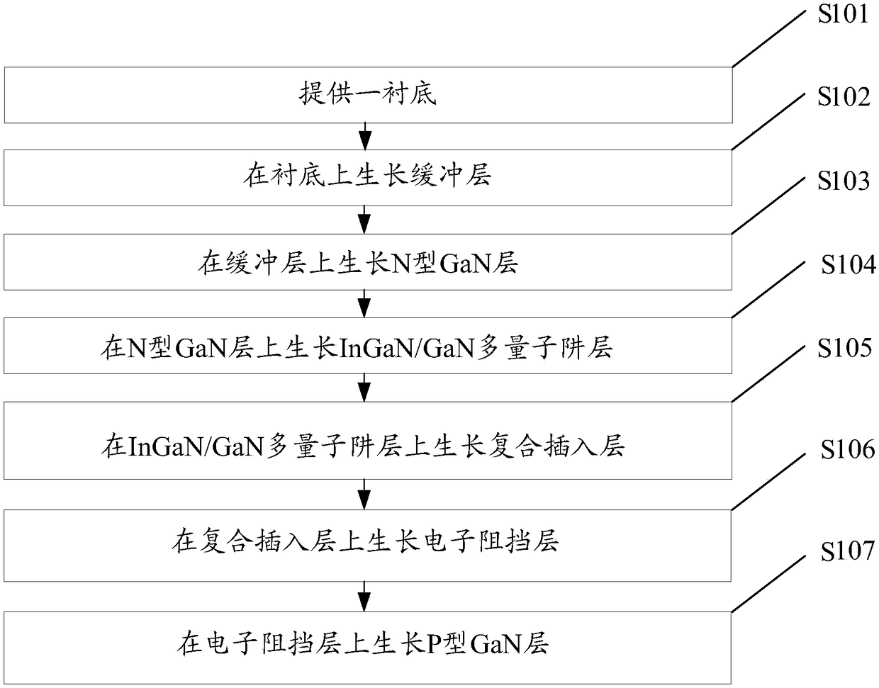
[0030] In order to make the object, technical solution and advantages of the present invention clearer, the implementation manner of the present invention will be further described in detail below in conjunction with the accompanying drawings.

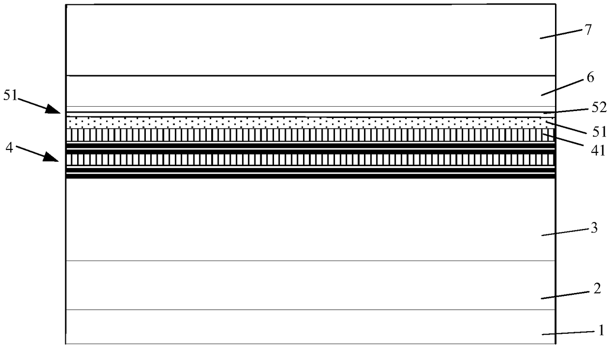
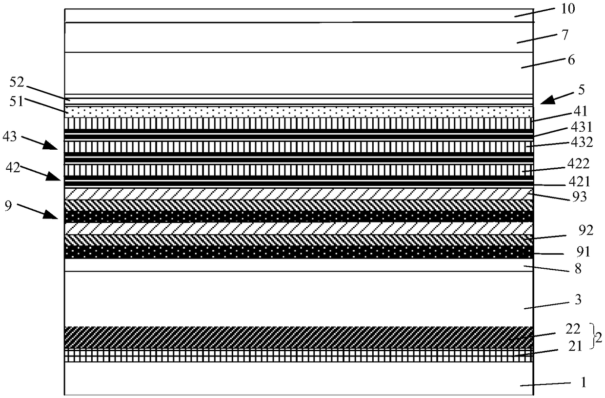
[0031] figure 1 It is a schematic structural diagram of an epitaxial wafer of a light emitting diode provided by an embodiment of the present invention. like figure 1 As shown, the epitaxial wafer includes a substrate 1 and a buffer layer 2, an N-type GaN layer 3, an InGaN / GaN multiple quantum well layer 4, a composite insertion layer 5, an electron blocking layer 6 and a P type GaN layer 7 .

[0032] Among them, the last GaN quantum barrier layer 41 of the InGaN / GaN multi-quantum well layer 4 stacked along the growth direction is doped with Al element, and the composite insertion layer 5 includes an AlN layer 51 and an InAlGaN layer 52 stacked in sequence, an AlN layer 51 and an InAlGaN layer Layers 52 are all doped with Mg element...


PUM


Abstract

The invention discloses an epitaxial wafer of a light emitting diode and a preparation method thereof, and belongs to the field of the light emitting diode manufacture. A combined inserting layer installed between an electron blocking layer and an InGaN/GaN multi-quantum well layer can be cooperated with the last one GaN quantum barrier layer doped with an Al element in the InGaN/GaN multi-quantumwell layer. The last one GaN quantum barrier layer doped with the Al element can play a partial effect of blocking an electron, the electron is blocked in the InGaN/GaN multi-quantum well layer, andan AlN layer and an InGaN layer with higher potential barriers in the combined inserting layer can also play the effect of blocking the electron. In addition, because a magnesium element is doped in the AlN layer and the InGaN layer, the AlN layer and the InGaN layer can be used as a hole source, the electron can be blocked in the InGaN/GaN multi-quantum well layer, and more holes can enter the InGaN/GaN multi-quantum well layer and are combined with the electrons so as to illuminate, and combination efficiency of the electrons and holes in the InGaN/GaN multi-quantum well layer is improved, so luminous efficiency of the light emitting diode is improved.

Description

technical field [0001] The invention relates to the field of light-emitting diode manufacturing, in particular to an epitaxial wafer of a light-emitting diode and a preparation method thereof. Background technique [0002] Light-emitting diodes are semiconductor diodes that can convert electrical energy into light energy. They have the advantages of small size, long life, and low power consumption. They are currently widely used in automotive signal lights, traffic lights, display screens, and lighting equipment. The epitaxial wafer is the basic structure for making light-emitting diodes. The structure of the epitaxial wafer includes a substrate and an epitaxial layer grown on the substrate. Among them, the structure of the epitaxial layer mainly includes: a buffer layer, an N-type GaN layer, an InGaN / GaN multi-quantum well layer, an electron blocking layer and a P-type GaN layer grown sequentially on the substrate. [0003] When a current flows in the epitaxial wafer, the ...

Claims


Application Information

Patent Timeline
Patent Type & Authority Applications(China)
IPC IPC(8): H01L33/06H01L33/14H01L33/00
CPCH01L33/0066H01L33/007H01L33/06H01L33/145
Inventor 吕蒙普叶芸郭炳磊胡加辉李鹏
Owner HC SEMITEK ZHEJIANG CO LTD
Why Eureka
Try Eureka