Novel package substrate and manufacturing method thereof

A technology for encapsulating substrates and manufacturing methods, which is applied in the fields of printed circuit manufacturing, multilayer circuit manufacturing, and photodevelopable thick films, etc., which can solve the problems of time-consuming and labor-intensive, high viscosity of glue, etc., so as to improve production efficiency and improve development Groove speed, convenient and quick effect of removing waste

Active Publication Date: 2014-11-19
安捷利美维电子(厦门)有限责任公司
View PDF7 Cites 2 Cited by
  • Summary
  • Abstract
  • Description
  • Claims
  • Application Information

AI Technical Summary

Problems solved by technology

In the existing circuit board slotting process, due to the high viscosity of the glue between the P sheet base material and the FR4 board, it is generally necessary to use a milling cutter to gradually cut off the waste from the inside to the outside, which is very time-consuming and laborious.

Method used


Image

  • Novel package substrate and manufacturing method thereof
  • Novel package substrate and manufacturing method thereof
  • Novel package substrate and manufacturing method thereof

Examples


Embodiment Construction

[0031] Such as Figure 1 to Figure 6 As shown, it is a manufacturing method of a novel package substrate according to the present invention, comprising the following steps:

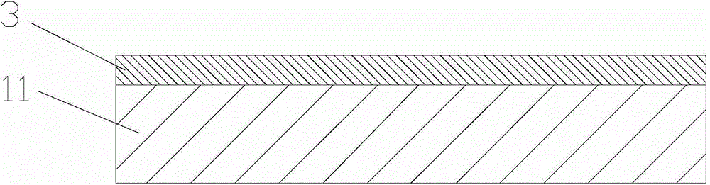
[0032] a. If figure 1 As shown, the first photosensitive dry film 3 is pasted on the upper surface of the first flame-resistant material plate 11 .

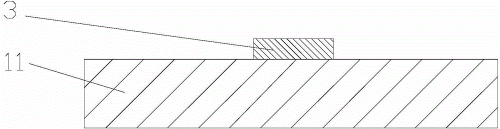
[0033] b. If figure 2 As shown, the first photosensitive dry film on the first flame-resistant material plate other than the predetermined groove position is removed by exposure and development.

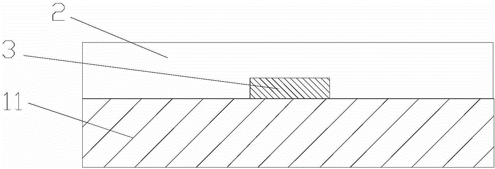
[0034] c. If image 3 As shown, a layer of P sheet substrate 2 is adhered on the upper surface of the first flame-resistant material plate 11 and the remaining first photosensitive dry film 3 .

[0035] d. If Figure 4 As shown, a second flame-resistant material plate 11 is bonded on the P sheet substrate.

[0036] e. If Figure 5 As shown, laser cutting is carried out from the upper surface of the second flame-resistant material plate 11 along the circumfe...


PUM


Abstract

The invention provides a manufacturing method of a novel package substrate. A first light-sensitive dry film adheres to a first flame-resistant material plate, then the first light-sensitive dry film is exposed and developed, a prepreg base material adheres to the first flame-resistant material plate at the moment, a second flame-resistant material plate adheres to the prepreg base material, and grooving is carried out. The invention further provides the novel package substrate. The first light-sensitive dry film is located between the first flame-resistant material plate and the prepreg base material after being exposed and developed, so no glue exists between the first flame-resistant material plate and the prepreg base material; thus, laser cutting can be adopted, the grooving speed is increased, waste is convenient and rapid to remove, and production efficiency is improved.

Description

technical field [0001] The invention relates to the field of packaging substrates, in particular to a novel packaging substrate and a manufacturing method thereof. Background technique [0002] Small size, light weight, and thin thickness are a development trend of electronic products. The components on the traditional circuit board are all arranged on the surface of the circuit board, which will inevitably increase the thickness of the circuit board, and at the same time cannot be used to manufacture multi-layer circuit boards. In order to make electronic products small and light, embedded multilayer circuit boards came into being. As the name implies, an embedded multilayer circuit board is a circuit board that embeds electronic components inside. [0003] Embedded circuit boards require slotting of the circuit board. In the existing circuit board slotting process, due to the high viscosity of the glue between the P sheet base material and the FR4 board, it is generally ...

Claims


Application Information

Patent Timeline
Patent Type & Authority Applications(China)
IPC IPC(8): H05K1/02H05K3/46
CPCH05K1/036H05K3/0035H05K2203/0191H05K2203/0384H05K2203/0514H05K3/46
Inventor 崔成强
Owner 安捷利美维电子(厦门)有限责任公司
Why Eureka
Try Eureka