Array substrate, manufacturing method thereof and display device

An array substrate and an array technology are applied in the fields of display devices, array substrates and preparation methods thereof, which can solve the problems of electric field interference, influence on the display effect of liquid crystal display devices, influence on the quality of display images, etc., so as to reduce the phenomenon of color mixing and light leakage, reduce The phenomenon of electric field interference, the effect of improving the display effect

Inactive Publication Date: 2014-11-26
BOE TECH GRP CO LTD
View PDF3 Cites 23 Cited by
  • Summary
  • Abstract
  • Description
  • Claims
  • Application Information

AI Technical Summary

Problems solved by technology

The resolution is defined as the number of pixel units per inch in the liquid crystal display device. In this way, the higher the resolution, the more the number of pixel units per inch, resulting in each liquid crystal display device. The size of the pixel unit is getting smaller and smaller, and the distance between the pixel electrodes in two adjacent pixel units is also getting smaller and smaller, such as figure 1 As shown, when a certain working voltage is applied to the pixel electrode 10, the electric field between two adjacent pixel electrodes 10 will be disturbed (as shown by the arrow in the figure), thereby affecting the quality of the displayed picture.
[0004] For example, if figure 2 As shown, when only the liquid crystal molecules 12 corresponding to a certain pixel unit (marked as a) are required to be deflected and the liquid crystal molecules 12 corresponding to another pixel unit (marked as b) adjacent to the pixel unit are not deflected, since the pixel unit The distance between a and pixel unit b is very small, so that the electric field between two adjacent pixel electrodes 10 interferes, resulting in liquid crystal molecules 12 between adjacent pixel unit a and pixel unit b, and pixel unit b The corresponding liquid crystal molecules 12 near the edge of the pixel unit a are deflected, so that the adjacent pixel units in the liquid crystal display device produce color mixing, light leakage and other phenomena, which affect the display effect of the liquid crystal display device

Method used


Image

  • Array substrate, manufacturing method thereof and display device
  • Array substrate, manufacturing method thereof and display device
  • Array substrate, manufacturing method thereof and display device

Examples


Embodiment 1

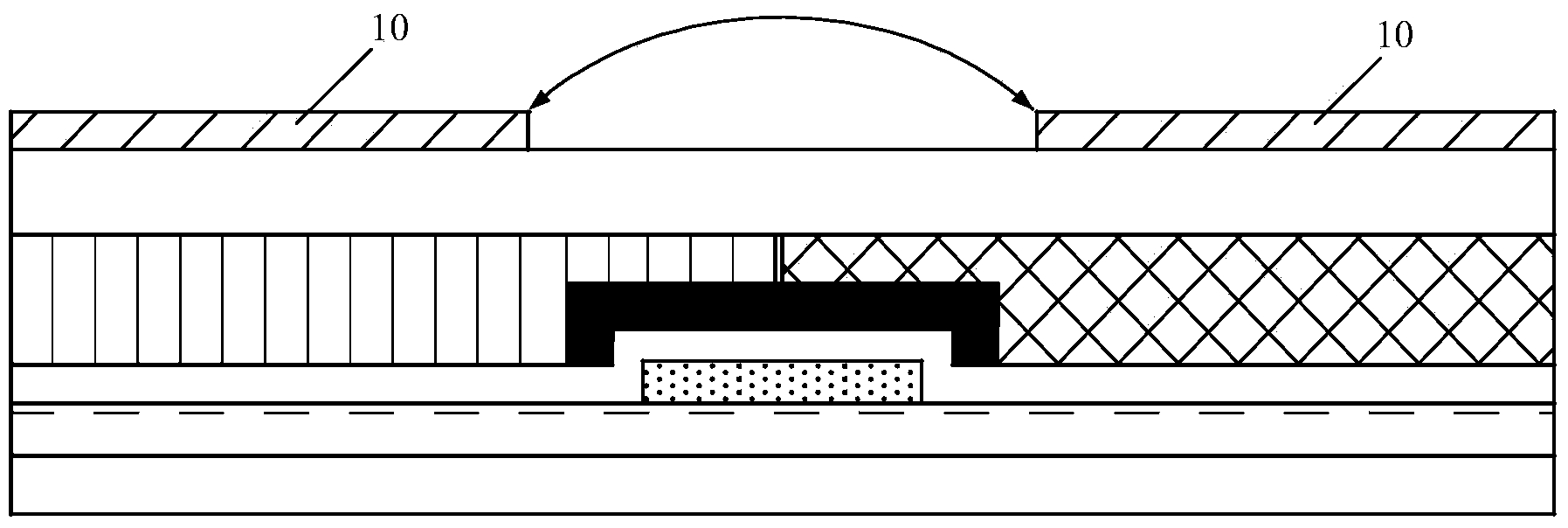
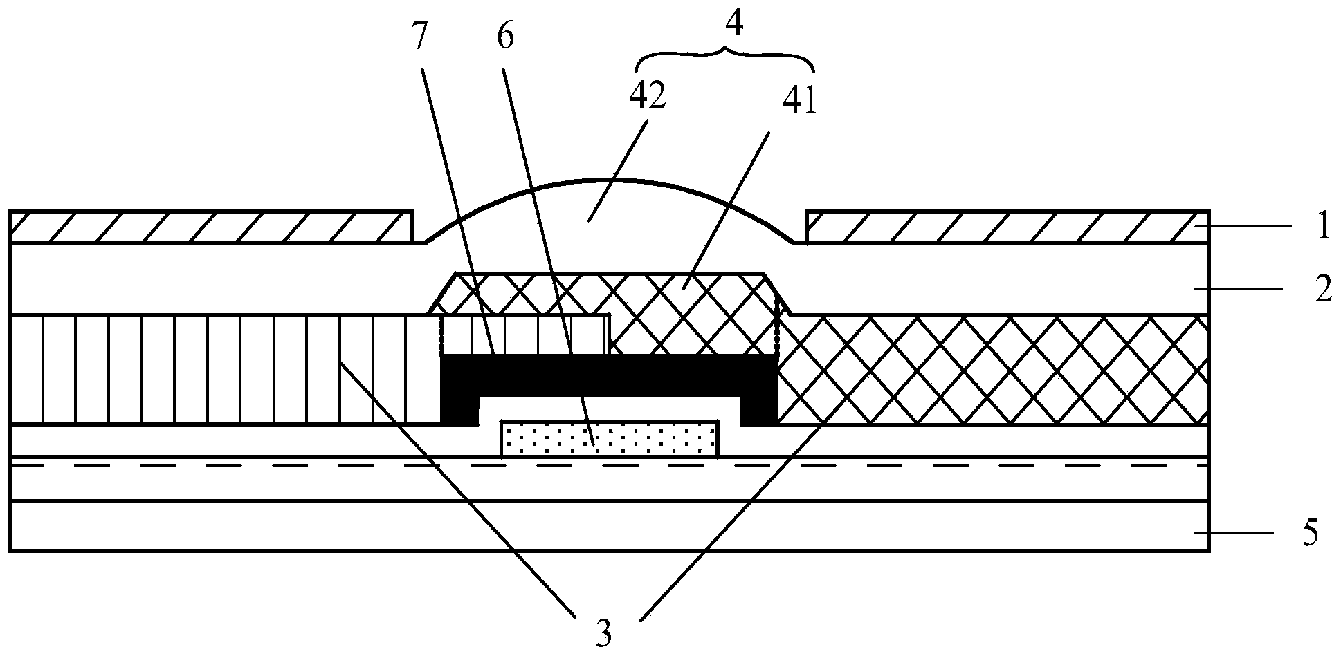
[0061] see image 3 , an embodiment of the present invention provides an array substrate, including: a plurality of pixel units arranged in an array, each pixel unit includes a first transparent electrode 1 and a color filter unit 3 oppositely arranged, wherein,

[0062] Edges of adjacent color filter units 3 are overlapped to form overlapping regions;

[0063] A first insulating layer 2 is arranged between the first transparent electrode 1 and the color filter unit 3, and a protrusion 4 is arranged between adjacent first transparent electrodes 1, and the protrusion 4 includes at least the corresponding part of the overlapping area, and the apex of the protrusion 4 is higher than the upper surface of the first transparent electrode 1 .

[0064] When the above-mentioned array substrate is applied in a display device, since the protrusion 4 is provided between the adjacent first transparent electrodes 1, the protrusion 4 can reduce the electric field interference phenomenon bet...

Embodiment 2

[0079] see image 3 and Figure 14 , an embodiment of the present invention provides a preparation method of an array substrate, the preparation method comprising:

[0080] 101. Form a color filter layer, the color filter layer includes a plurality of color filter units 3 arranged in an array, the colors of adjacent color filter units 3 are different, and the colors of adjacent color filter units 3 Edge overlap setting to form an overlapping area;

[0081] 102. Form a first insulating layer 2 and a protrusion 4 on the color filter layer, where the protrusion 4 includes at least a part of the first insulating layer 2 corresponding to the overlapping area;

[0082] 103. Form a plurality of first transparent electrodes 1 arranged in an array on the first insulating layer 2, each first transparent electrode 1 corresponds to a color filter unit 3; protrusions 4 are located on adjacent first transparent electrodes 1, and the apex of the protrusion 4 is higher than the upper surfa...


PUM

PropertyMeasurementUnit
heightaaaaaaaaaa

Abstract

The invention discloses an array substrate, a manufacturing method of the array substrate and a display device, and relates to the technical field of display. The array substrate comprises a plurality of pixel units arranged in an array shape, each pixel unit comprises a first transparent electrode and a color light filtering unit which are arranged oppositely, the edges of the adjacent color light filtering units are overlapped, and an overlapping area is formed. First insulation layers are arranged between the first transparent electrodes and the color light filtering units, protrusions are arranged between the adjacent first transparent electrodes, the protrusions at least comprise parts, corresponding to the overlapping area, in the first insulation layers, and peaks of the protrusions are higher than the upper surfaces of the first transparent electrodes. When the array substrate is applied to the display device, the interference of electric fields between the adjacent first transparent electrodes can be reduced, color mixing and light leakage between the adjacent pixel units are reduced, and the display effect of the display device is improved.

Description

technical field [0001] The present invention relates to the field of display technology, in particular to an array substrate, a preparation method thereof, and a display device. Background technique [0002] With the development and progress of thin film transistor liquid crystal display (TFT-LCD Display) technology, liquid crystal display devices have replaced cathode ray tube display devices and become mainstream display devices in the daily display field. [0003] At present, in order to continuously improve the quality of images displayed by liquid crystal display devices, the resolution thereof is continuously improved, in an effort to provide consumers with clearer and more realistic display images. The resolution is defined as the number of pixel units per inch in the liquid crystal display device. In this way, the higher the resolution, the more the number of pixel units per inch, resulting in each liquid crystal display device. The size of the pixel unit is getting...

Claims


Application Information

Patent Timeline
Patent Type & Authority Applications(China)
IPC IPC(8): G02F1/1343G02F1/1333
CPCG02F1/133345G02F1/133514G02F1/136209G02F1/136222G02F1/1335G02F1/1362G02F1/133512G02F1/133516G02F1/13439G02F1/136286H01L27/124H01L27/1262
Inventor 姚琪张锋曹占锋舒适
Owner BOE TECH GRP CO LTD
Why Eureka
Try Eureka