

Bearing substrate and manufacturing method thereof
A technology for carrying substrates and manufacturing methods, applied in multilayer circuit manufacturing, printed circuits connected with non-printed electrical components, electrical connection printed components, etc., can solve the problem that users cannot easily distinguish between connection pads and wiring, oxidation , affecting electrical performance and other issues, to achieve the effect of avoiding oxidation, maintaining electrical performance, and improving joint reliability
- Summary
- Abstract
- Description
- Claims
- Application Information
AI Technical Summary
Problems solved by technology
Method used
Image

Examples
Embodiment Construction
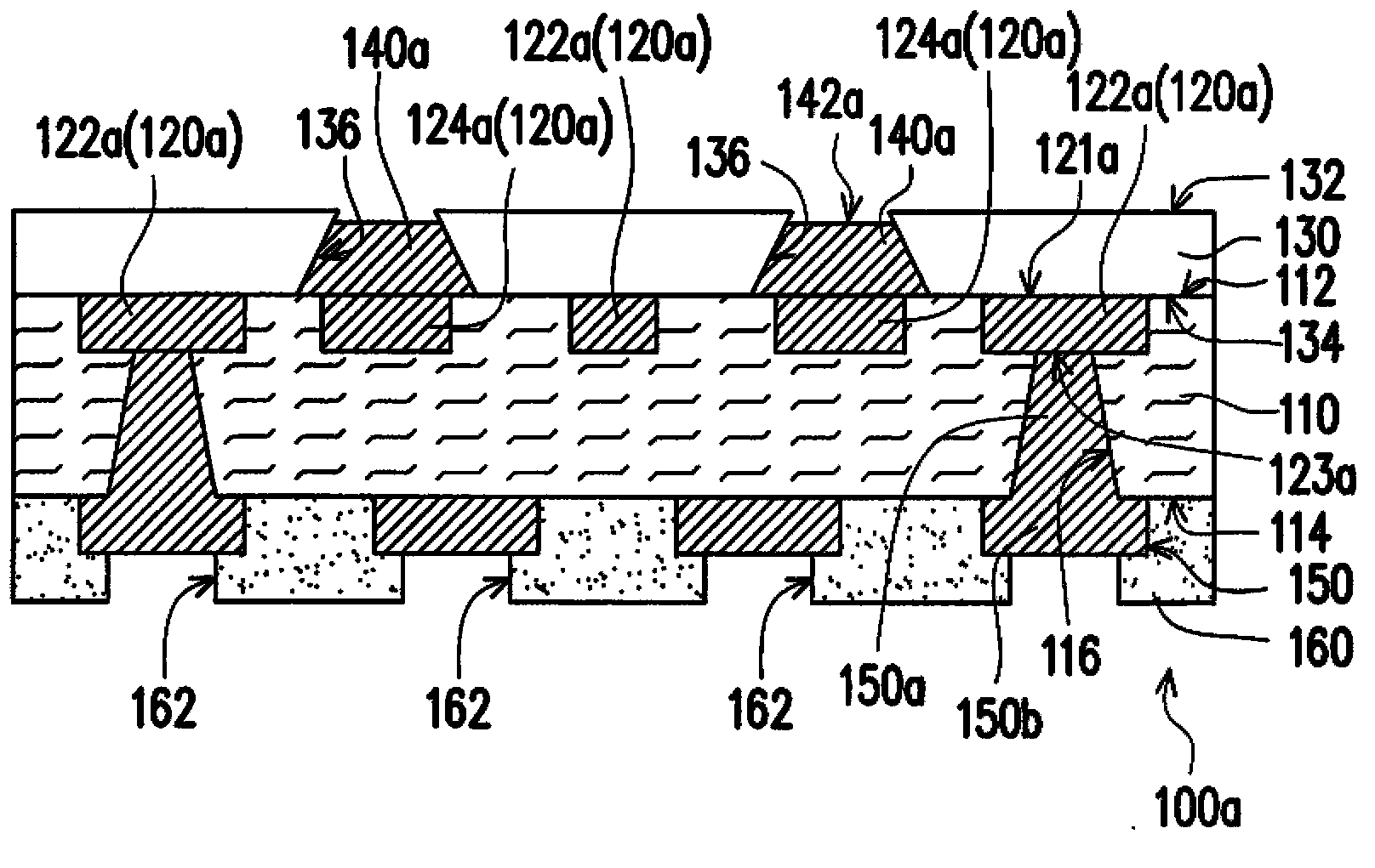
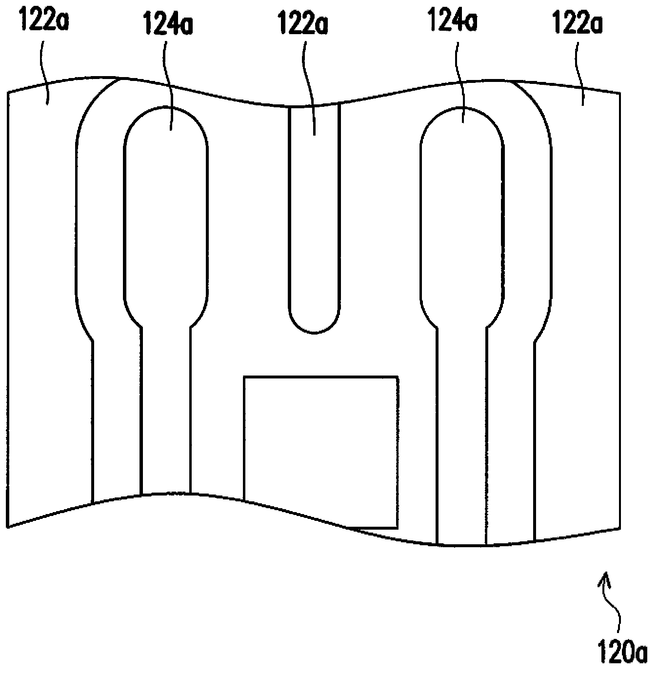
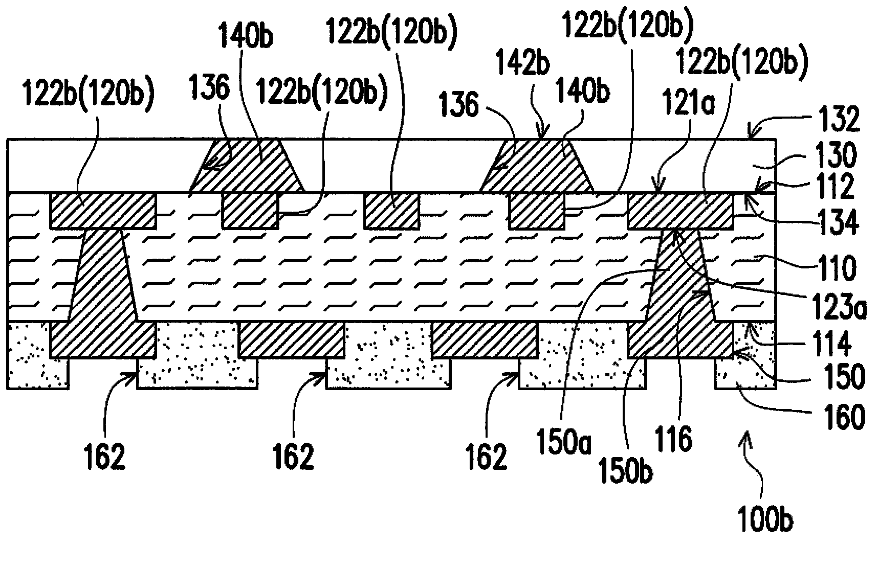
[0069] Figure 1A A schematic cross-sectional view of a carrier substrate according to an embodiment of the present invention is shown. Figure 1B shown as Figure 1A A schematic top view of the circuit layer. Please refer to Figure 1A , in this embodiment, the carrier substrate 100a includes a dielectric layer 110 , a first circuit layer 120a , an insulating layer 130 , a plurality of conductive blocks 140a and a first conductive structure 150 . In detail, the dielectric layer 110 has two opposite surfaces 112, 114 and a plurality of blind holes 116 ( Figure 1A Two are shown schematically in ). The first wiring layer 120a is embedded in the surface 112 of the dielectric layer 110 and has two opposite surfaces 121a, 123a, wherein the surface 121a is exposed on the surface 112 of the dielectric layer 110 . The blind hole 116 extends from the surface 114 to the first wiring layer 120a and exposes a portion of the surface 123a of the first wiring layer 120a. The insulating la...
PUM
 Abstract
Description
Claims
Application Information