
Manufacturing method for bend-resistant bus card casing
A manufacturing method and technology for a bus card, applied in the field of mobile communications, can solve the problems of chip damage, being bent, easy to lose, etc., and achieve the effects of improving buffer protection, slowing down distortion, and preventing chip damage
- Summary
- Abstract
- Description
- Claims
- Application Information
AI Technical Summary
Problems solved by technology
Method used
Image

Examples
Embodiment 1
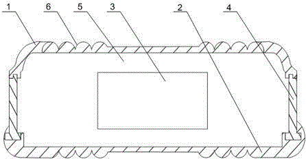
[0024] Such as figure 1 As shown, this embodiment includes the following steps:
[0025] (A) forming an upper shell 1 and a lower shell 2 capable of engaging with each other by injection molding in a mold;
[0026] (B) installing a filler 5 in the lower case 2, and placing the chip 3 at the center of the lower case 2;
[0027] (C) The upper case 1 and the lower case 2 are connected and matched by the rubber block 4, and then the upper case 1 and the lower case 2 are bonded and sealed by an adhesive.
[0028] In the above steps, the upper casing 1 and the lower casing 2 are connected to each other through rubber blocks 4 to form a closed cavity, and a chip 3 is fixed in the cavity, and a filler 5 is provided between the chip 3 and the cavity, Two elastic connecting portions 6 are provided on the outer walls of the upper casing 1 and the lower casing 2 respectively, and the width of the connecting portions 6 is 1 / 4 of the total width of the upper casing 1 . The work of the pr...
Embodiment 2
[0031] Such as figure 1 As shown, in this embodiment, on the basis of Embodiment 1, the four connecting parts 6 are arranged symmetrically on the outer walls of the upper casing 1 and the lower casing 2 centering on the cavity. Four elastic connecting parts 6 are symmetrically distributed in pairs on the upper casing 1 and the lower casing 2. When the surface of the IC card is impacted by an external force, the elastic recovery of the connecting parts 6 can be superimposed to the maximum, and the direction is consistent with the direction of the external force. On the contrary, to the greatest extent offset the distortion caused by the external force acting on the card surface.
[0032] Preferably, the cross section of the connecting portion 6 is wavy. The connection portion 6 with a wavy cross section can generate a relatively large amount of deformation per unit area, which can further improve the buffer protection of the upper shell 1 and the lower shell 2 .
PUM
 Abstract
Description
Claims
Application Information