Display panel and display device

A display panel and display device technology, applied in the fields of instruments, nonlinear optics, optics, etc., can solve problems such as performance degradation, thin film transistor performance degradation, and off-state current rise

Active Publication Date: 2014-12-17
BOE TECH GRP CO LTD +1
View PDF5 Cites 12 Cited by
  • Summary
  • Abstract
  • Description
  • Claims
  • Application Information

AI Technical Summary

Problems solved by technology

[0003] On this basis, due to the existence of the light-induced attenuation effect (Stabler-Wronski Effect), after a long-term use of the display panel, the light entering its interior will inevitably irradiate the active layer of the thin film transistor , leading to performance degradation of the thin film transistor
[0004] For example, for an active matrix liquid crystal display device, after the light emitted by the backlight enters the liquid crystal display panel, it will inevi

Method used


Image

  • Display panel and display device
  • Display panel and display device
  • Display panel and display device

Examples


Embodiment Construction

[0025] The following will clearly and completely describe the technical solutions in the embodiments of the present invention with reference to the accompanying drawings in the embodiments of the present invention. Obviously, the described embodiments are only some, not all, embodiments of the present invention. Based on the embodiments of the present invention, all other embodiments obtained by persons of ordinary skill in the art without making creative efforts belong to the protection scope of the present invention.

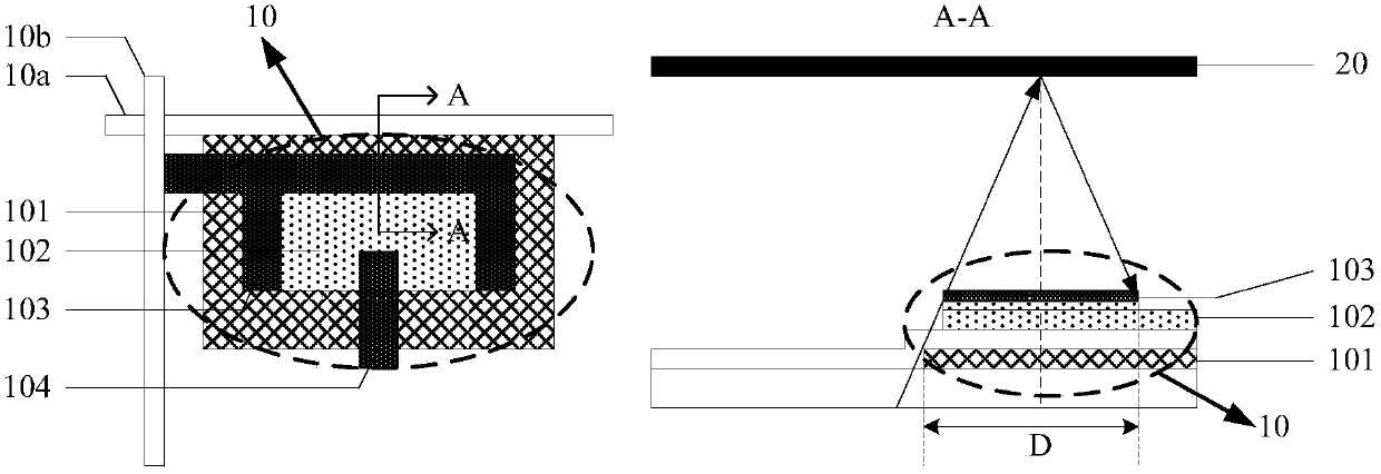
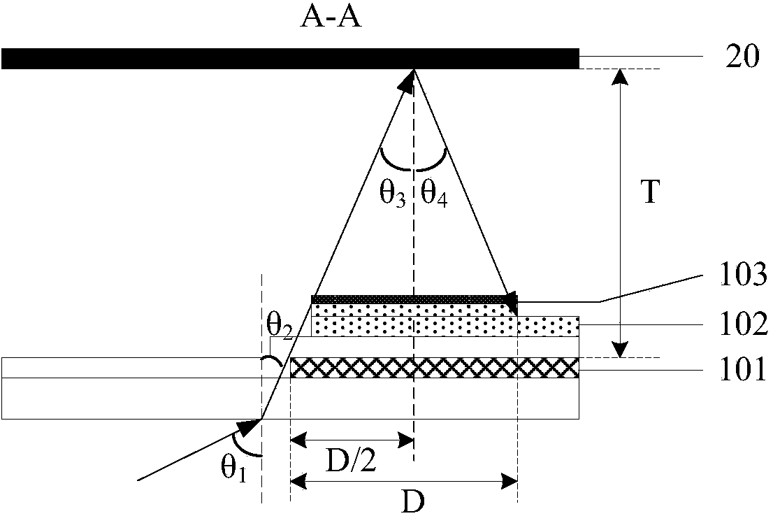
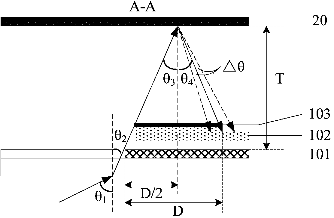
[0026] Embodiments of the present invention provide a display panel, such as figure 1 As shown, it includes a thin film transistor 10 and a black matrix 20 arranged oppositely; the thin film transistor 10 may include a gate 101, a source 103 and a drain 104 arranged on a base substrate, and an active layer between the two. layer 102; the gate 101 is located on the side of the active layer 102 away from the black matrix 20, and the source 103 and the drain 104 ...


PUM


Abstract

The embodiment of the invention discloses a display panel and a display device, relates to technical field of display, and aims to prevent light rays reflected by a block matrix from being irradiated onto the active layer of a thin film transistor in order to delay the performance deterioration of the thin film transistor and ensure the display quality. The display panel comprises the thin film transistor and the black matrix which are arranged oppositely, a grid line and a data line, wherein the thin film transistor comprises a grid electrode, a source electrode, a drain electrode and an active layer; the grid electrode is positioned on one side, which is far away from the black matrix, of the active layer; the source electrode and the drain electrode are positioned on one side, which is close to the black matrix, of the active layer; the source electrode is positioned between the drain electrode and the grid line; the side edge, which faces away from the grid electrode, of the grid line is taken as a first edge; the source electrode is close to the drain electrode, and the side edge, which is parallel to the grid line, of the source electrode is taken as a second edge; the distance between the first edge and the second edge is greater than or equal to a preset distance D, so that light rays entering from one side of the thin film transistor are prevented from being irradiated onto the surface of the active layer after being reflected by the black matrix. The display panel is applied to manufacturing of the display device.

Description

technical field [0001] The present invention relates to the field of display technology, in particular to a display panel and a display device. Background technique [0002] At present, the driving modes of display panels can be mainly divided into two modes: active matrix type and passive matrix type; among them, the active matrix type display panel needs to realize the control of each pixel unit through thin film transistors. [0003] On this basis, due to the existence of the light-induced attenuation effect (Stabler-Wronski Effect), after a long-term use of the display panel, the light entering its interior will inevitably irradiate the active layer of the thin film transistor , thereby degrading the performance of the thin film transistor. [0004] For example, for an active matrix liquid crystal display device, after the light emitted by the backlight enters the liquid crystal display panel, it will inevitably irradiate the active layer of the thin film transistor thr...

Claims


Application Information

Patent Timeline
IPC IPC(8): G02F1/1362G02F1/1368G02F1/1335
Inventor 李升玄喻娟邵喜斌刘冬
Owner BOE TECH GRP CO LTD
Why Eureka
Try Eureka