Method for manufacturing afebrile array wave-guide grating based on flat-plate wave-guide movement

A technology of arrayed waveguide grating and slab waveguide, which is applied in the coupling direction of optical waveguide, can solve the problems of spectrum deterioration, high device cost, and limited freedom of re-coupling, etc., and achieves simple and easy device fabrication, simplified process steps, and reduced The effect of device cost

Active Publication Date: 2009-04-29
GUANGXUN SCI & TECH WUHAN
View PDF12 Cites 12 Cited by
  • Summary
  • Abstract
  • Description
  • Claims
  • Application Information

AI Technical Summary

Problems solved by technology

[0012] Realizing the athermal characteristic of AWG, there are other schemes, which are limited to a small number of literature reports. These methods are not described here because of their poor practicability.
[0013] Existing technologies based on slab waveguide movement such as figure 1 , 2 As shown, the following patents Patent No.: US 6470119 B1, Patent No.: US 6798948 B2, Patent No.: US 6865323 B2, Patent No.: US 6961498 B2, Patent No.: US 6563986 B2, Patent No.: US 6735364 B2, Patent No.: US 8626332 B2, Patent No.: US 6954566 B2, Patent No.: US 6975793 B2, Patent No.: US 6668116 B2, Patent No.: US 6668117 B2, Patent No.: US 6490395 B1 , WO 2006/073229 A1, CN1302131A, and CN1392961A are athermal arrayed waveguide grating schemes based on the movement of slab waveguides. The characteristics of the scheme are summarized as follows: 1) There is a substrate 11 under the relatively

Method used


Image

  • Method for manufacturing afebrile array wave-guide grating based on flat-plate wave-guide movement
  • Method for manufacturing afebrile array wave-guide grating based on flat-plate wave-guide movement
  • Method for manufacturing afebrile array wave-guide grating based on flat-plate wave-guide movement

Examples


Embodiment Construction

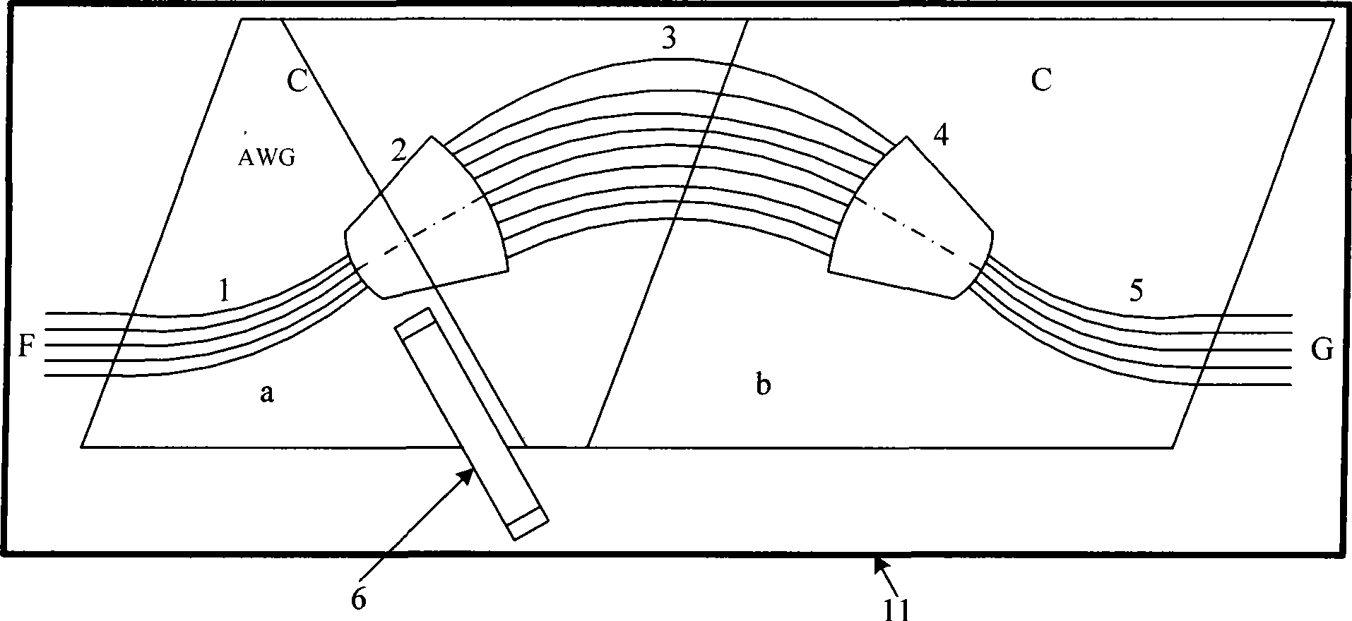
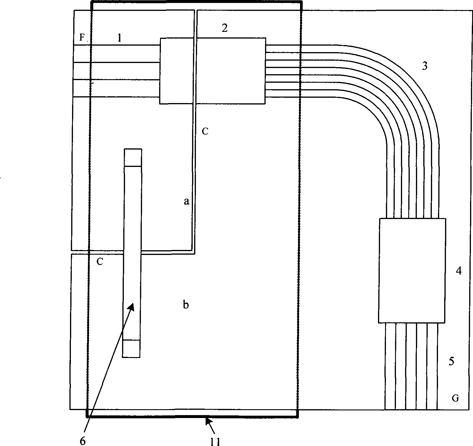
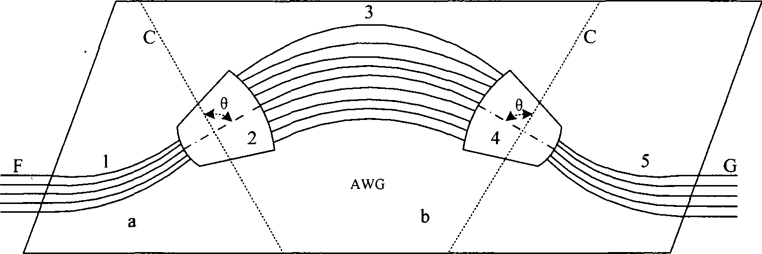
[0043] The method for manufacturing the athermal arrayed waveguide grating based on the movement of the slab waveguide of the present invention will be described in detail below in conjunction with the accompanying drawings of the embodiments.

[0044] The manufacturing method of the athermal arrayed waveguide grating based on the movement of the slab waveguide of the present invention is to cut along the cutting line on the input slab waveguide 2 on the ordinary silicon-based silicon dioxide arrayed waveguide grating (AWG) chip made by adopting the planar optical waveguide technology. C or the cutting line C on the output slab waveguide 4 divides the AWG chip into a first part a and a second part b, the first part a includes a part of the input waveguide 1 and the input slab waveguide 2, and the second part b includes the The remaining part, the arrayed waveguide 3, the output slab waveguide 4 and the output waveguide 5; the temperature compensation rod 6 is placed across the ...


PUM


Abstract

The invention discloses a method for manufacturing an afebrile array wave-guide grating based on flat-plate wave-guide movement, which comprises the following steps that a common silicon-based silica array wave-guide grating chip is divided into a first part and a second part along a cutting line for inputting a flat-plate wave guide or a cutting line for outputting the flat-plate wave guide on the array wave-guide grating chip; a temperature compensating rod spans the cutting line of the array wave-guide grating chip and is fixed with the surfaces of the first part and the second part of the array wave-guide grating chip; and the expansion and contraction of the temperature compensating rod drive the first part and the second part to move relatively, so as to compensate wavelength shift caused by the temperature and manufacture the afebrile array wave-guide grating. The method doses not adopt a substrate. The first part a and the second part b are placed on a six-axes precision fine tuning bracket to be fully and freely adjusted in six directions; the device cost is reduced; the processing steps are simplified to the maximum degree so that the manufacture of the device is easy to implement; deterioration of the performance of the device is reduced to the maximum degree; and the stability is strong.

Description

technical field [0001] The invention relates to a temperature-insensitive arrayed waveguide grating. In particular, it relates to the manufacture of an athermal arrayed waveguide grating based on the movement of a slab waveguide, which uses the thermal expansion and contraction of the temperature compensation rod to drive the relative movement of the two parts a and b of the arrayed waveguide grating chip, thereby compensating the wavelength drift caused by temperature. method. Background technique [0002] As the continuous growth of IP data services and the emergence of various broadband access services have brought about unlimited demands on bandwidth, Dense Wavelength Division Multiplexing (DWDM) technology has been flourishing. The multiplexer and demultiplexer are the key devices in the DWDM system. At present, there are devices with various structures that can realize the wavelength division multiplexing function, such as thin film interference filters, acousto-optic...

Claims


Application Information

Patent Timeline
IPC IPC(8): G02B6/34
Inventor 周天宏马卫东
Owner GUANGXUN SCI & TECH WUHAN
Why Eureka
Try Eureka