Thin film transistor, display substrate and display device

A technology for thin film transistors and display substrates, used in transistors, semiconductor devices, electric solid state devices, etc., can solve problems such as poor electrode disconnection

Active Publication Date: 2014-12-17
BOE TECH GRP CO LTD
View PDF4 Cites 19 Cited by
  • Summary
  • Abstract
  • Description
  • Claims
  • Application Information

AI Technical Summary

Problems solved by technology

[0005] Embodiments of the present invention provide a thin film transistor, a display substrate, and a display device, which can improve the problem of poor disconnection of electrodes formed subsequently in via holes

Method used


Image

  • Thin film transistor, display substrate and display device
  • Thin film transistor, display substrate and display device
  • Thin film transistor, display substrate and display device

Examples


Embodiment Construction

[0024] The following will clearly and completely describe the technical solutions in the embodiments of the present invention with reference to the accompanying drawings in the embodiments of the present invention. Obviously, the described embodiments are only some, not all, embodiments of the present invention. Based on the embodiments of the present invention, all other embodiments obtained by persons of ordinary skill in the art without making creative efforts belong to the protection scope of the present invention.

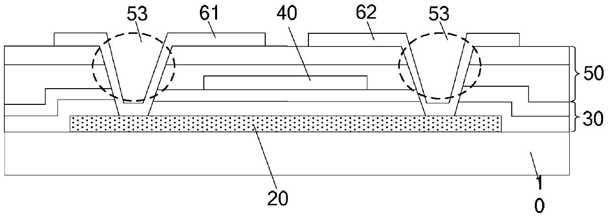
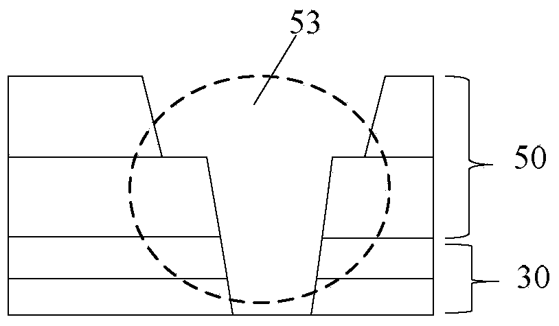
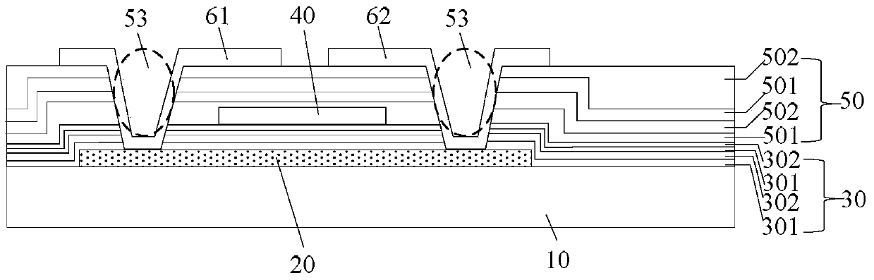
[0025] An embodiment of the present invention provides a thin film transistor, such as Figure 3 to Figure 7 As shown, the thin film transistor includes an active layer 20, a gate insulating layer 30, a gate electrode 40, an interlayer dielectric layer 50, a source electrode 61, and a drain electrode 62 that are sequentially arranged on a base substrate 10. The source electrode 61 and The drain electrode 62 is respectively connected to the active layer 20 thro...


PUM


Abstract

The invention relates to the technical field of display, provides a thin film transistor, a display substrate and a display device and aims to solve the problem of bad disconnection of follow-up electrodes in via holes. The thin film transistor comprises an active layer, a gate insulator, a grid electrode, an interlevel dielectric, a source electrode and a drain electrode, and the active layer, the gate insulator, the grid electrode, the interlevel dielectric, the source electrode and the drain electrode are sequentially arranged on a substrate. The source electrode and the drain electrode are respectively connected with the active layer through via holes exposed outside the active layer; the grid insulator at least comprises two silicon oxide layers and two silicon nitride layers, and the interlevel dielectric at least comprises four silicon oxide layers and four silicon nitride layers; all silicon oxide layers and silicon nitride layers of the gate insulator and the interlevel dielectric are arranged at intervals, and one side, away from the substrate, of each via hole is larger than one side, close to the substrate, of each via hole. The thin film transistor is applicable to manufacturing of the display device and the display substrate with the thin film transistor.

Description

technical field [0001] The invention relates to the field of display technology, in particular to a thin film transistor, a display substrate and a display device. Background technique [0002] With the improvement of people's living standards, display devices such as mobile phones, cameras, computers, and televisions are widely used by people. A thin film transistor (Thin Film Transistor, TFT for short), as one of the important components of these devices, directly affects the display effect of the display device. [0003] Such as figure 1 As shown, one type of thin film transistor includes: an active layer 20, a gate insulating layer 30, a gate electrode 40, an interlayer dielectric layer 50, and a source electrode 61 and a drain electrode 62 sequentially arranged on a base substrate 10; Wherein, the source electrode 61 and the drain electrode 62 are respectively connected to the active layer 20 through the interlayer dielectric layer 50 and the via hole 53 on the gate i...

Claims


Application Information

Patent Timeline
Patent Type & Authority Applications(China)
IPC IPC(8): H01L29/786H01L29/06H01L27/12
CPCH01L27/1214H01L29/42364H01L29/42384H01L29/786H01L29/4908H01L27/1244H01L27/1248H01L27/12H01L29/06H01L27/124
Inventor 王祖强刘建宏
Owner BOE TECH GRP CO LTD
Why Eureka
Try Eureka