A led vertical chip structure with special roughened morphology and its preparation method

A chip structure and morphology technology, applied in the direction of electrical components, circuits, semiconductor devices, etc., can solve the problem of low light extraction efficiency, achieve the effect of improving luminous efficiency, simple process, and improving light extraction efficiency

Inactive Publication Date: 2017-02-15
ENRAYTEK OPTOELECTRONICS
View PDF9 Cites 0 Cited by
  • Summary
  • Abstract
  • Description
  • Claims
  • Application Information

AI Technical Summary

Problems solved by technology

[0005] The purpose of the present invention is to provide a vertical structure LED and its preparation method to solve the problem of low light extraction efficiency of vertical structure LED in the prior art

Method used


Image

  • A led vertical chip structure with special roughened morphology and its preparation method
  • A led vertical chip structure with special roughened morphology and its preparation method
  • A led vertical chip structure with special roughened morphology and its preparation method

Examples


Embodiment Construction

[0051] The present invention will be described in further detail below in conjunction with the accompanying drawings and specific embodiments. Advantages and features of the present invention will be apparent from the following description and claims. It should be noted that the drawings are all in a very simplified form and use imprecise ratios, which are only used to facilitate and clearly assist the purpose of illustrating the embodiments of the present invention.

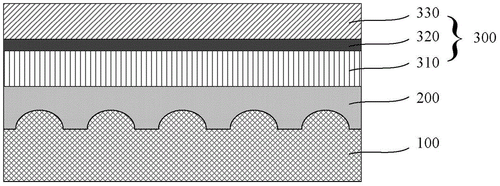
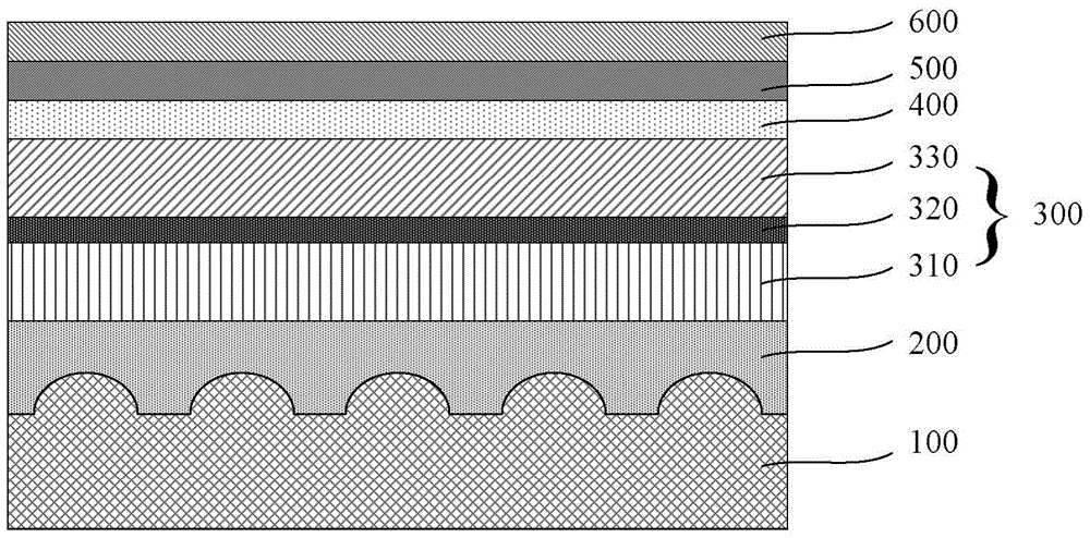
[0052] The present invention provides a LED vertical chip structure with special roughened morphology, such as Figure 8As shown, the LED vertical chip structure includes: a conductive support substrate 700, a metal bonding electrode layer 600 formed on the surface of the conductive support substrate 700, and a metal reflective electrode formed on the surface of the metal bonding electrode layer 600 layer 500 , the contact layer 400 formed on the surface of the metal reflective electrode layer 500 , the epitaxi...


PUM


Abstract

A method for improving luminous efficiency of an LED in a vertical structure. First, an LED vertical chip structure with a special coarsening morphology is provided, and micron-scale holes (311) are formed in the surface of an epitaxial structure layer (300) and submicron-scale holes (312) are formed at the bottom of the micron-scale holes. The light emitting surface structure can increase the emission probability of light inside a device, and can greatly improve the light emission efficiency. Also provided is a preparation method for the chip structure. Micron-scale holes (311) are formed in an epitaxial structure layer (300) by stripping a growth substrate (100) with micron-scale bumps, and submicron-scale holes (312) are formed at the bottom of the micron-scale holes (311) by means of etching. The method is simple in process, can be applied to large-scale industrial production, and can greatly improve the luminous efficiency of the LED in the vertical structure.

Description

technical field [0001] The invention relates to the field of semiconductors, in particular to an LED vertical chip structure with a special roughened appearance and a preparation method thereof. Background technique [0002] In terms of the structure of LED (Light-Emitting Diode, light-emitting diode), it can be divided into front structure, flip structure and vertical structure. Vertical structure LEDs can effectively solve the key problems of low heat dissipation and current blocking in front-mounted structure LEDs and flip-chip structure LEDs, improve the luminous efficiency and light intensity density of LEDs, and have good heat dissipation, can carry large currents, and high luminous intensity. Due to the advantages of low power consumption and long life, it is widely used in general lighting, landscape lighting, special lighting, automotive lighting and other fields. It is receiving more and more attention and research from the industry, and it is an inevitable trend i...

Claims


Application Information

Patent Timeline
Patent Type & Authority Patents(China)
IPC IPC(8): H01L33/20H01L33/00
CPCH01L33/0075H01L33/0093H01L33/22H01L33/405H01L33/647H01L2933/0016H01L33/00
Inventor 童玲张琼吕孟岩张宇李起鸣
Owner ENRAYTEK OPTOELECTRONICS
Why Eureka
Try Eureka