

Touch display panel, preparation method thereof and touch display device
A touch display panel and display area technology, which is applied in the fields of instruments, computing, electrical and digital data processing, etc., can solve the problem of reducing the touch performance and display performance of the touch display device, and the signal transmission circuit of the touch display panel cannot work normally. And other issues
- Summary
- Abstract
- Description
- Claims
- Application Information
AI Technical Summary
Problems solved by technology
Method used
Image

Examples
preparation example Construction
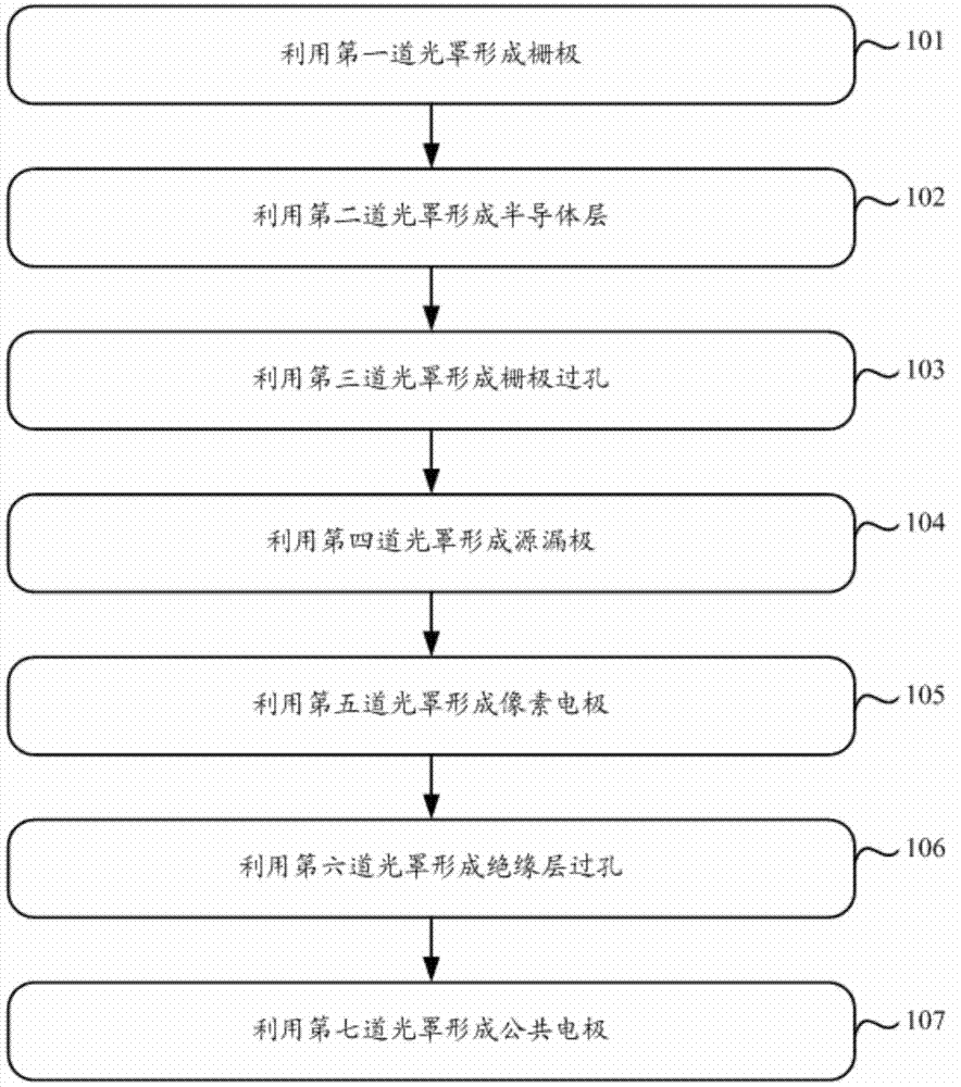
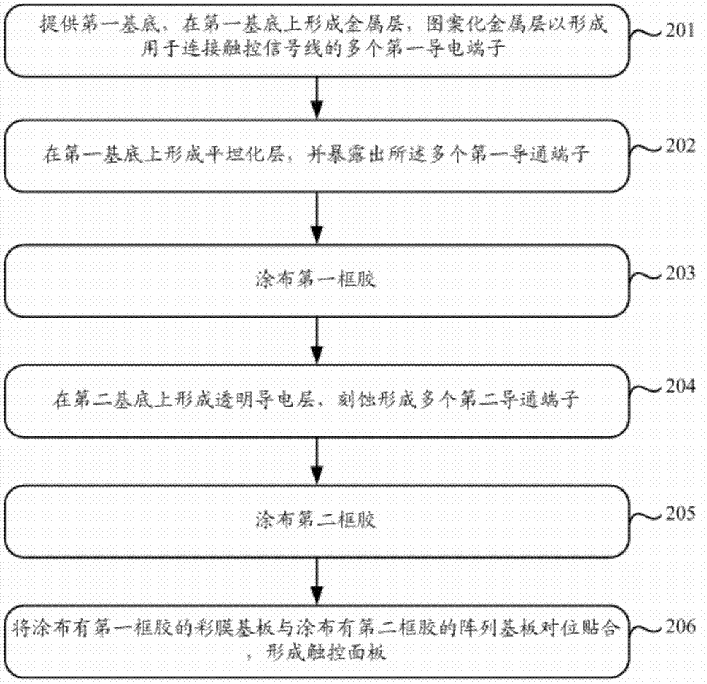
[0078] It should be noted that, for the convenience of description, the first substrate in the embodiment of the present invention is an example of a color filter substrate, but the example of the first substrate as a color filter substrate is only an example, not a limitation. In actual work, the first substrate is still It may be a cover plate or a packaging cover plate. An embodiment of the present invention provides a method for manufacturing a touch display panel, including:
[0079] providing a first substrate and a second substrate;
[0080] Coating a conductive first adhesive material on the first substrate, coating an insulating second adhesive material on the second substrate; or coating an insulating second adhesive material on the first substrate, Coating a conductive first adhesive material on the second substrate; wherein, the second adhesive material is in the shape of a frame, and the projection of the first adhesive material on the first substrate is located ...
example 1
[0126] Considering the cumbersome preparation process of the 7mask process of the array substrate, in order to simplify the process flow, the present invention adopts the 5mask process or the 6mask process. In the existing coating method, a sealing frame including conductive balls is coated on the array substrate in one stroke, which will cause unnecessary discharge or short circuit on the color filter substrate side. Therefore, in order to avoid affecting the normal operation of peripheral circuits, and to ensure the normal conduction between the first conductive terminal and the second conductive terminal without affecting the production capacity, the present invention sets the first conductive terminal and the second conductive terminal at the first The projection on the substrate (color filter substrate) is located outside the projection range of the insulating second adhesive material on the first substrate (color filter substrate), or the first conductive terminal and the...
example 2
[0129] In view of the practicability and better technical effect of the solution of Example 1, the embodiment of the present invention is improved based on the solution of Example 1, and the specific improvements are as follows.
[0130] Considering that the flattening layer of the color filter substrate is likely to damage the peripheral traces of the touch capacitor during the etching process, in order to ensure normal circuit operation, it is possible to avoid etching the peripheral trace area of the touch capacitor To protect the peripheral wiring of the touch capacitor on the color filter substrate side.
[0131] Such as Figure 10(a) ~ 10(d)As shown, it is a simple schematic diagram of the lamination of the color filter substrate C2 and the array substrate T. In FIG. The plurality of first conductive terminals 301' are used to connect touch signal lines; the planarization layer 302' does not etch the peripheral circuit area, so the projection of the planarization laye...
PUM
 Abstract
Description
Claims
Application Information