Method for analyzing defects

A defect analysis and barrier layer technology, which is applied in analyzing materials, using radiation for material analysis, and using wave/particle radiation for material analysis, etc. Defect analysis, the effect of extended capabilities

Inactive Publication Date: 2014-12-24
WUHAN XINXIN SEMICON MFG CO LTD
View PDF5 Cites 12 Cited by
  • Summary
  • Abstract
  • Description
  • Claims
  • Application Information

AI Technical Summary

Problems solved by technology

[0006] The above two patents do not record the relevant technical features of the defect analysis method of the present invention

Method used


Image

  • Method for analyzing defects
  • Method for analyzing defects
  • Method for analyzing defects

Examples


Embodiment Construction

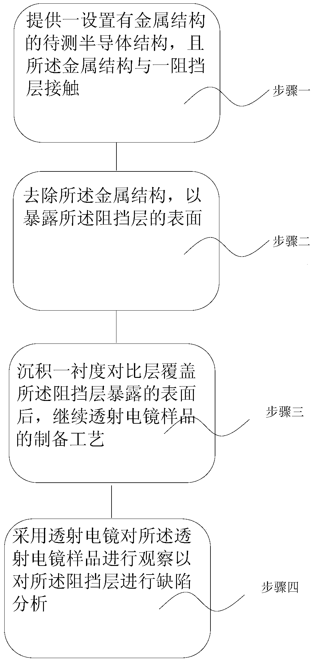
[0027] The present invention will be further described below in conjunction with the accompanying drawings and specific embodiments, but not as a limitation of the present invention.

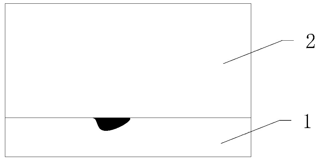
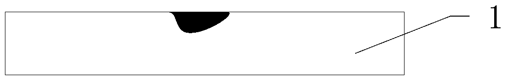
[0028] Such as figure 1 As shown, the present embodiment relates to a defect analysis method, comprising the following steps:

[0029] In step 1, a semiconductor structure to be tested is provided with a metal structure 2, and the metal structure 2 is in contact with the barrier layer 1. In an embodiment of the present invention, several semiconductor structures have been formed in the semiconductor structure to be tested (not shown in the figure). shown), the semiconductor structure to be tested may include a substrate and a gate structure covering the surface of the substrate, etc., because the specific structure of the semiconductor structure to be tested is not the focus of the improvement of the present invention, so it will not be described in detail here, and for the sake of To describe ...


PUM


Abstract

The invention relates to the technical field of semiconductor defect analysis, in particular to a method for analyzing defects. The method comprises the steps that after a metal structure of a semiconductor structure to be detected is removed, a contrast comparison layer which has large the difference from a barrier layer in material atomic number is deposited on the barrier layer, then a conventional transmission electron microscope sample is prepared, and a transmission electron microscope is used for observing the transmission electron microscope sample to conduct defect analysis on the barrier layer. Due to the fact that the barrier is covered with the contrast comparison layer which has the large difference from the barrier layer in material atomic number, the defects of the barrier layer can be clearly observed in the transmission electron microscope, and therefore defect analysis can be accurately conducted. According to the method for actively improving the image contrast of the transmission electron microscope to analyze micro defects, the capacity of micro defect failure analysis can be further expanded, and therefore better technical support is provided for manufacture procedure technologies.

Description

technical field [0001] The invention relates to the technical field of semiconductor defect analysis, in particular to a defect analysis method. Background technique [0002] In transmission electron microscopy (TEM) sample analysis, TEM image contrast can be used to distinguish different materials. The contrast is mainly determined by the thickness of the sample and the nature of the material. The current method to distinguish between two similar materials is to adjust the thickness of the sample and increase the weight of the observed material as much as possible to make the contrast obvious. [0003] As process dimensions decrease, the size of process defects also decreases. When the size of the defect is as small as about 20nm or even smaller, it becomes necessary to use transmission electron microscopy to analyze the defect. However, in the process of TEM sample preparation (focused ion beam cutting method), it is easy to miss the defect because it is difficult to id...

Claims


Application Information

Patent Timeline
Patent Type & Authority Applications(China)
IPC IPC(8): H01L21/66H01L21/02G01N23/02
CPCH01L22/12G01N23/2202G01N23/2251H01L22/24H01L22/30
Inventor 刘君芳李桂花仝金雨郭伟李品欢
Owner WUHAN XINXIN SEMICON MFG CO LTD
Why Eureka
Try Eureka