Array substrate, manufacturing method thereof and display device

A technology for array substrates and display devices, which is applied in semiconductor/solid-state device manufacturing, semiconductor devices, electrical components, etc., can solve problems such as lowering production costs and failure to display sub-pixel functions normally, so as to reduce production costs, ensure quality, and avoid The effect of defective

Active Publication Date: 2014-12-24
BOE TECH GRP CO LTD +1
View PDF4 Cites 6 Cited by
  • Summary
  • Abstract
  • Description
  • Claims
  • Application Information

AI Technical Summary

Problems solved by technology

[0004] Embodiments of the present invention provide an array substrate, a manufacturing method thereof, and a display device, which solves the problem that in existing high-definition display devices, the drain electrode is connected to the common electrode layer, which leads to the connection between the common electrode layer and the pixel electrode layer, and the sub-pixel function cannot be achieved. Normal display, the problem of forming dark spots, ensures the quality of the product, reduces the waste of production materials, and greatly reduces the production cost

Method used


Image

  • Array substrate, manufacturing method thereof and display device
  • Array substrate, manufacturing method thereof and display device
  • Array substrate, manufacturing method thereof and display device

Examples


Embodiment Construction

[0046] The following will clearly and completely describe the technical solutions in the embodiments of the present invention with reference to the accompanying drawings in the embodiments of the present invention. Obviously, the described embodiments are only some, not all, embodiments of the present invention. Based on the embodiments of the present invention, all other embodiments obtained by persons of ordinary skill in the art without making creative efforts belong to the protection scope of the present invention.

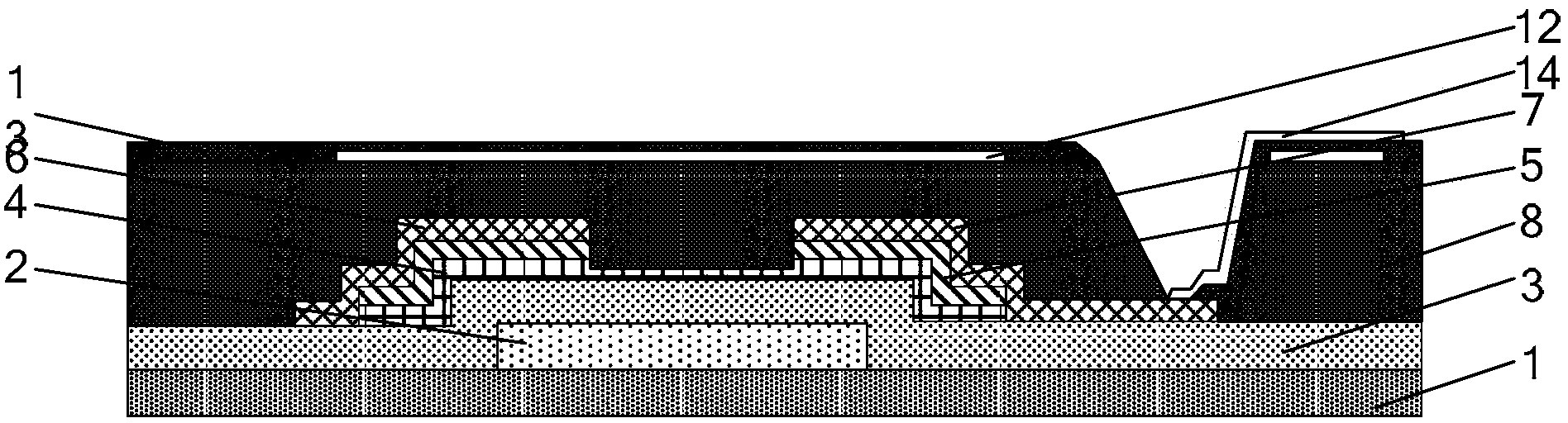
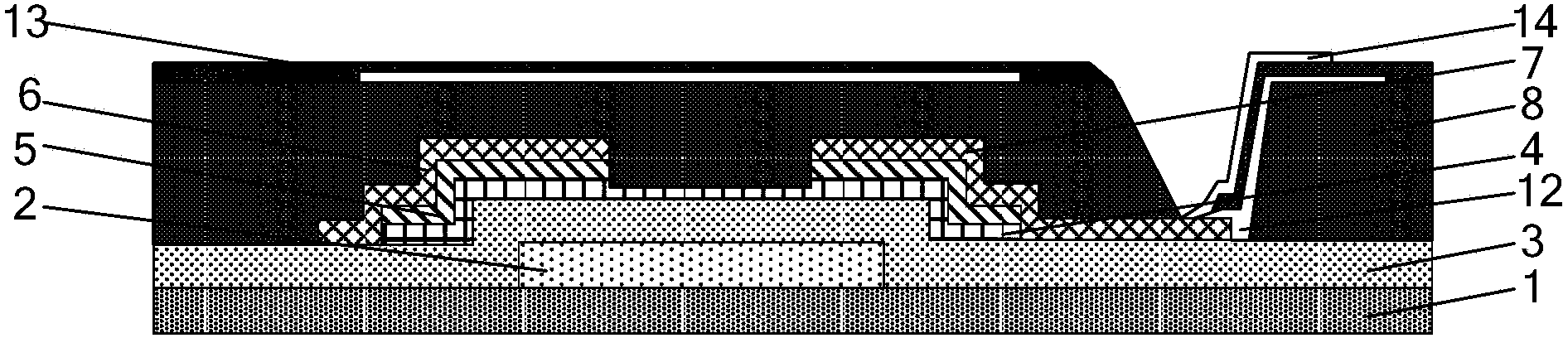
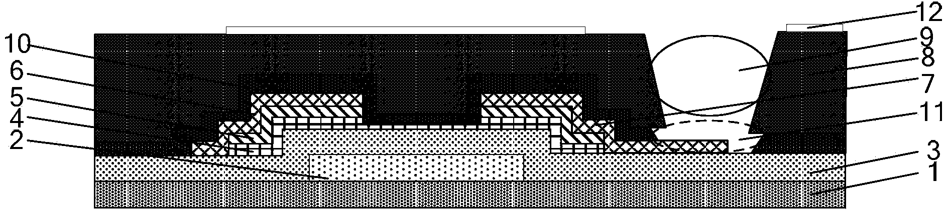
[0047] An embodiment of the present invention provides an array substrate, referring to image 3 As shown, the array substrate includes: a substrate 1, a gate 2, a gate insulating layer 3, an active layer 4, an ohmic contact layer 5, a source 6, a drain 7, an organic resin layer 8, and an organic resin layer formed on the organic resin layer 8. The common electrode layer 12, the first via hole 9 and the isolation layer 10 are formed on the organic resin layer ...


PUM


Abstract

The invention provides an array substrate, a manufacturing method of the array substrate and a display device and relates to the technical field of liquid crystal display panel manufacture. The problems that a drain electrode and a common electrode layer of an existing high-definition display device are communicated, so that the common electrode layer and a pixel electrode layer are communicated, the sub-pixel function can not be achieved normally, and dark spots are generated are solved. Product quality is guaranteed, the waste of production materials is reduced, and production cost is reduced. The array substrate comprises a substrate body, a source electrode, a drain electrode, an organic resin layer and a common electrode layer formed on the organic resin layer. A first passing hole is formed in the organic resin layer, an isolation layer is arranged on the source electrode and the drain electrode and covers the substrate body, and the isolation layer is completely covered with the organic resin layer. A second passing hole communicated with the first passing hole to expose part of the drain electrode is formed in the isolation layer, wherein the size of the firs passing hole is larger than that of the first passing hole. The array substrate, the manufacturing method of the array substrate and the display device are applied to the technical field of display panel manufacture.

Description

technical field [0001] The present invention relates to the field of display technology, in particular to an array substrate, a manufacturing method thereof, and a display device. Background technique [0002] With the continuous development of liquid crystal display technology, the resolution requirements of display devices are getting higher and higher, and currently full high-definition display has become the mainstream. In order to realize full high-definition display devices, such as figure 1 As shown in , an organic resin layer 8 needs to be formed on the source electrode 6 and the drain electrode 7 to reduce the power consumption of the array substrate and increase the aperture ratio. At the same time, it is necessary to make a via hole to connect the drain electrode to the pixel electrode layer, and finally generate a voltage difference between the common electrode layer and the pixel electrode layer to ensure the normal display of the sub-pixel function. [0003] ...

Claims


Application Information

Patent Timeline
IPC IPC(8): H01L27/12H01L21/77
CPCH01L21/31116Y02P80/30H01L27/1244H01L27/1248H01L27/1259H01L21/77H01L27/12H01L21/31138H01L21/76816H01L27/1262
Inventor 姜晓辉阎长江张家祥
Owner BOE TECH GRP CO LTD
Why Eureka
Try Eureka