
CMOS (complementary metal oxide semiconductor) image sensor capable of being used in multiple working modes

An image sensor and working mode technology, which is applied in image communication, color TV parts, TV system parts, etc., can solve the problems of not taking into account multi-spectral output and large quantum efficiency at the same time, to increase charge transfer efficiency, Enhanced potential gradient, high quantum efficiency output effect

Active Publication Date: 2014-12-24
UNITED MICROELECTRONICS CENT CO LTD
View PDF2 Cites 2 Cited by
  • Summary
  • Abstract
  • Description
  • Claims
  • Application Information

AI Technical Summary

Problems solved by technology

[0007] In order to solve the problem that the existing CMOS image sensor cannot take into account the multi-spectral output and high quantum efficiency at the same time, the present invention proposes a CMOS image sensor that can be used in multiple working modes

Method used


Image

  • CMOS (complementary metal oxide semiconductor) image sensor capable of being used in multiple working modes
  • CMOS (complementary metal oxide semiconductor) image sensor capable of being used in multiple working modes
  • CMOS (complementary metal oxide semiconductor) image sensor capable of being used in multiple working modes

Examples


Embodiment Construction

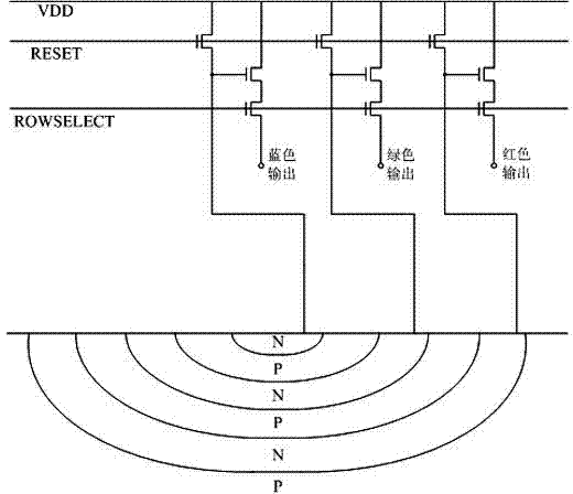
[0039] attached figure 1 It is a schematic diagram of the vertically stacked pixel structure of the prior art CMOS image sensor. It can be seen from the figure that the prior art vertically stacked pixel structure is based on 3T pixels, adopts a stacked structure, and uses three layers of PN junctions with different depths to sense three different colors of light. The photo-generated charges of the photosensitive layer are output in three ways through three different sets of source followers, reset transistors and line selection transistors corresponding to the three photosensitive layers, that is, blue, green, and red outputs, so as to realize visible light color output.

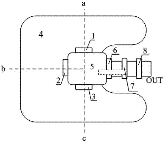
[0040] attached figure 2 It is a schematic top view of a CMOS image sensor with a three-layer stacked structure pixel that can be used in multiple working modes in the present invention, with the attached image 3 is attached figure 2 Schematic diagram of the section along the b-a tangent line, with F...


PUM


Abstract

The invention provides a CMOS (complementary metal oxide semiconductor) image sensor capable of being used in multiple working modes and aims to solve the problem that an CMOS image sensor in the prior art cannot take both multispectral output and high quantum efficiency into consideration. The CMOS image sensor is structured on the basis of 4T pixel of surface clamping and comprises three transmission grids, a photoelectric diode, a floating node, a resetting tube resetting grid, a source tracker and a selectron, the photoelectric diode adopts a three-N-buried-layer vertical stacked structure, each N buried layer senses illumination of different wavebands and is correspondingly connected with one transmission grid, three N buried layers share the floating node, and the CMOS image sensor can be in different working modes by differently sequencing the transmission grids, the resetting tube resetting grid and the selectron. The CMOS image sensor has the advantages that multispectral selection output of a single pixel can be realized, and high-quantum-efficiency output of pixels can be realized.

Description

[0001] field of invention [0002] The invention relates to CMOS image sensor design technology, in particular to a CMOS image sensor that can be used in multiple working modes. Background technique [0003] CMOS image sensors have been developed by leaps and bounds due to their low cost, high integration, and higher and higher imaging quality, and are widely used in machine vision, security monitoring, portable applications, medical, military and other fields. CMOS image sensors in the prior art are mainly active pixel image sensors APS, including 3T, 4T, and 5T pixels. Since CMOS image sensors with 3T pixels and 5T pixels have disadvantages such as inability to perform correlated double sampling, CMOS image sensors with 4T pixels have become mainstream products. [0004] The quantum efficiency of a pixel refers to the ratio between the photo-generated charges collected by the photodiode and the photons injected into the pixel. The more photo-generated electrons, the full...

Claims


Application Information

Patent Timeline
Patent Type & Authority Applications(China)
IPC IPC(8): H01L27/146H04N5/374
Inventor 李毅强吴治军刘昌举李明邓光平李梦萄
Owner UNITED MICROELECTRONICS CENT CO LTD
Learn More