Display panel provided with pixel defining layer and manufacturing method of pixel defining layer

A pixel-defining layer and display panel technology, applied in semiconductor/solid-state device manufacturing, electrical components, electrical solid-state devices, etc., can solve the problems of uneven brightness, leakage, and uneven film in the pixel area

Inactive Publication Date: 2014-12-24
BOE TECH GRP CO LTD
View PDF5 Cites 85 Cited by
  • Summary
  • Abstract
  • Description
  • Claims
  • Application Information

AI Technical Summary

Problems solved by technology

However, due to the difference in surface energy between the ink drop and the pixel defining layer 20, the large slope angle of the PDL, and the drying behavior of the ink drop itself, it is easy to form an uneven film with thin edges and thick middle after the ink drop dries, especially in the The film thickness varies greatly at the edge of the pixel area, as figure 1 The area A circled by the dotted line in the center is shown
As

Method used


Image

  • Display panel provided with pixel defining layer and manufacturing method of pixel defining layer
  • Display panel provided with pixel defining layer and manufacturing method of pixel defining layer
  • Display panel provided with pixel defining layer and manufacturing method of pixel defining layer

Examples


no. 1 example

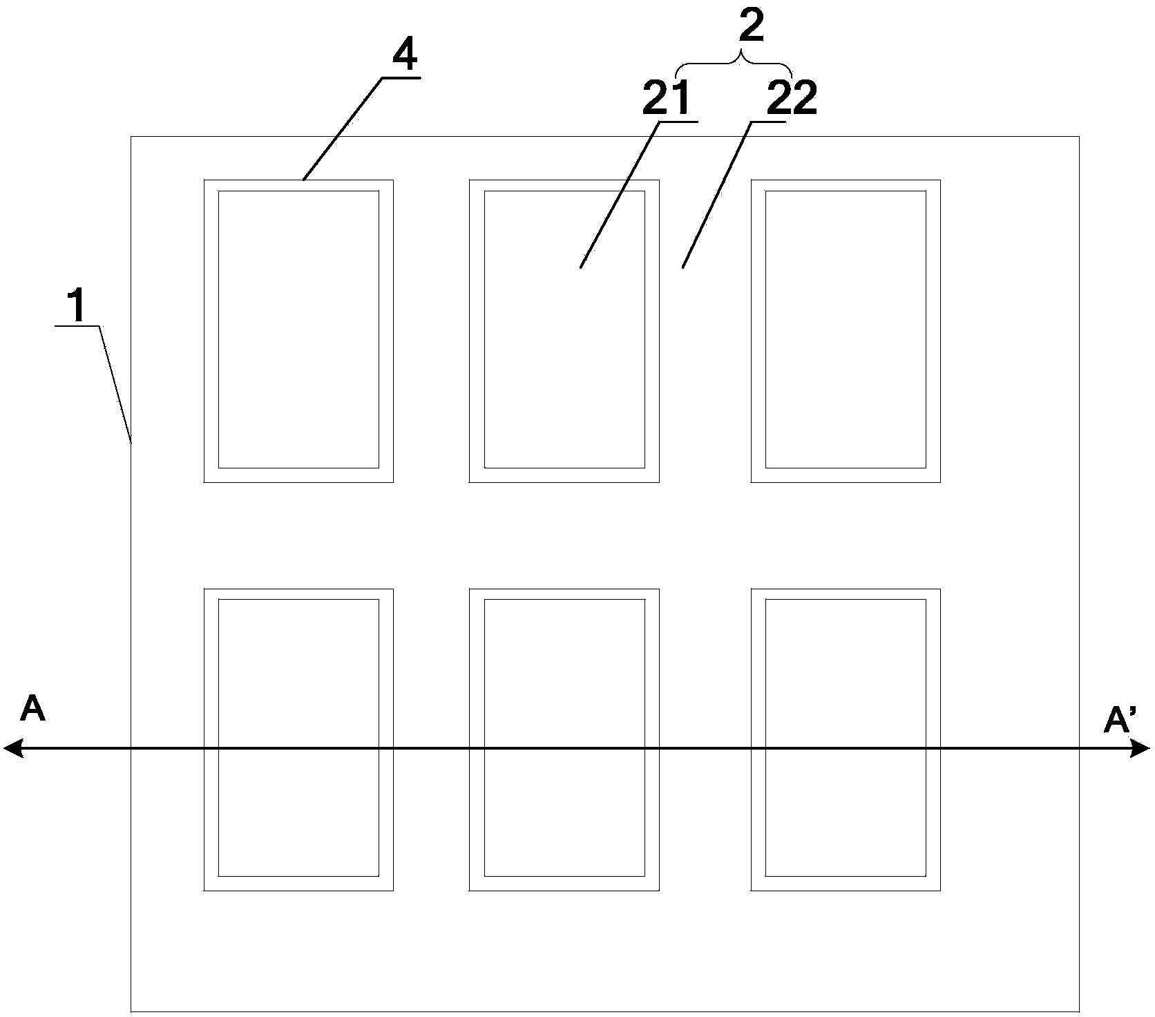
[0036] According to a first embodiment of the present invention there is provided a display panel with a pixel defining layer, figure 2is a schematic plan view of a display panel with a pixel-defining layer, in figure 2 Among them, a plurality of pixel regions 4 are formed on the substrate 1, and the plurality of pixel regions 4 are distributed in a matrix. Here, only part of the pixel regions are shown for brevity. The pixel defining layer 2 is formed on the substrate 1, and the pixel defining layer 2 includes multiple An opening 21 and a pixel separator 22 surrounding the opening to define the pixel region 4 .

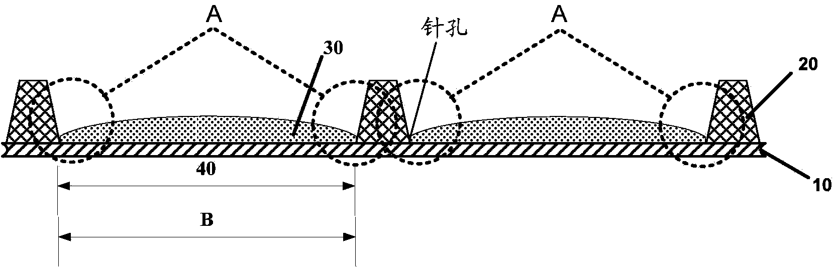
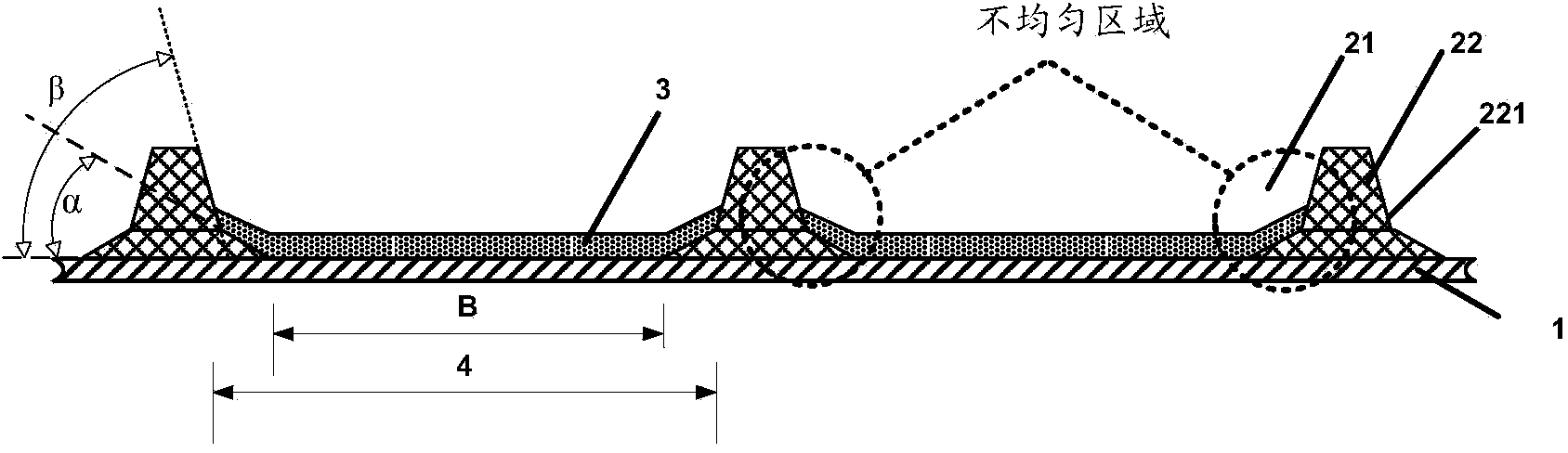
[0037] image 3 is along figure 2 The cross-sectional view taken by the line A-A' in image 3 As shown, the sidewall 221 of the pixel separator 22 for defining the pixel region, that is, the sidewall facing the pixel region 4 , is formed with a slope angle of the upper portion greater than that of the lower portion. Exemplarily, in the pixel region 4 defined b...

no. 2 example

[0055] A second embodiment according to the present invention provides a method for manufacturing the pixel defining layer according to the first embodiment.

[0056] Step S101 , providing a substrate.

[0057] The substrate in the embodiment of the present invention is the substrate before forming the pixel defining layer, which may be a base substrate or a structure obtained by forming multiple thin films or layers on the base substrate. The base substrate may be glass, silicon wafer, quartz or the like. For example, if Figure 7 As shown, the substrate includes a base substrate 11 and an anode layer 15 formed on the base substrate 11 . As an example, in the following descriptions, the substrate 1 including the base substrate 11 and the anode layer 15 formed on the base substrate 11 is taken as an example for illustration.

[0058] Step S102 , forming a pixel defining material layer on the substrate 1 .

[0059] In this step, the method for forming the pixel-defining mat...


PUM

PropertyMeasurementUnit
Heightaaaaaaaaaa
Thicknessaaaaaaaaaa

Abstract

The embodiment of the invention provides a display panel provided with a pixel defining layer and a manufacturing method of the pixel defining layer. The display panel provided with the pixel defining layer comprises a substrate, multiple pixel areas distributed on the substrate in a matrix and the pixel defining layer arranged on the substrate. The pixel defining layer comprises multiple openings and a pixel separation body defining the openings in an enclosed mode and limiting the pixel areas, and the slope angle of the upper portion of the side wall, used for limiting the pixel area, of the pixel separation body is larger than the slope angle of the lower portion of the side wall, used for limiting the pixel area, of the pixel separation body.

Description

technical field [0001] Embodiments of the invention relate to a display panel with a pixel defining layer and a manufacturing method of the pixel defining layer. Background technique [0002] Organic electroluminescent displays have the advantages of self-luminescence, fast response, wide viewing angle, high brightness, bright colors, thin and light, etc. Therefore, organic electroluminescent display technology has become an important display technology. [0003] At present, the methods for forming the organic electroluminescent layer of the organic electroluminescent display include: 1. The evaporation process is adopted. This method is suitable for small organic molecules. It is characterized in that the formation of the organic electroluminescent layer does not require a solvent, and the film thickness is uniform. However, the equipment investment is large, the material utilization rate is low, and it is not suitable for the production of large-scale products; 2. The solu...

Claims


Application Information

Patent Timeline
IPC IPC(8): H01L27/32H01L51/52H01L51/56
CPCH10K59/122H10K71/13
Inventor 王辉锋刘则
Owner BOE TECH GRP CO LTD
Why Eureka
Try Eureka