PCB structure

A PCB board and plug-in hole technology, which is applied in the field of PCB board structure with plug-in holes, can solve problems such as unqualified products, high difficulty, and weak welding

Inactive Publication Date: 2014-12-24
NEW H3C TECH CO LTD
View PDF3 Cites 1 Cited by
  • Summary
  • Abstract
  • Description
  • Claims
  • Application Information

AI Technical Summary

Problems solved by technology

Therefore, for PCB boards with fine-pitch plug-ins, under the condition that the printing area of ​​solder paste and the printing thickness of solder paste cannot be changed arbitrarily during actual use, it may not be able to meet the requirements between each plug-in and plug-in hole. The amount of solder paste required, and then there are ...

Method used


Image

  • PCB structure
  • PCB structure
  • PCB structure

Examples


Embodiment Construction

[0025] The present invention will be described in detail below in conjunction with specific embodiments shown in the accompanying drawings. However, these embodiments do not limit the present invention, and any structural, method, or functional changes made by those skilled in the art according to these embodiments are included in the protection scope of the present invention.

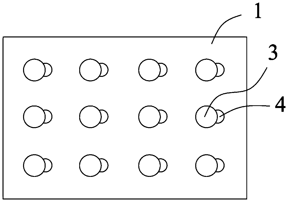
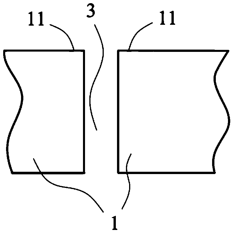
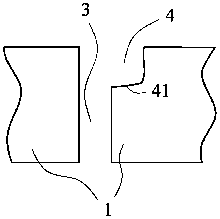
[0026] Please refer to figure 1 , figure 2 with Figure 4a-Figure 4c ,in, figure 1 It is a schematic diagram of the overall structure of a PCB board structure of the present invention; figure 2 It is a schematic cross-sectional view of not offering a storage tank for the PCB board structure of the present invention; Figure 4a It is a schematic cross-sectional view of printed solder of a PCB board structure of the present invention; Figure 4b It is a schematic cross-sectional view of a plug-in plug-in plug-in hole of a PCB board structure of the present invention; Figure 4c It is a schematic ...


PUM


Abstract

The invention discloses a PCB structure. A PCB is provided with a plurality of plugging piece holes allowing plugging pieces to be installed. A storage tank used for storing welding flux is formed in the position of at least one plugging piece hole of the PCB. The storage tanks are communicated with the plugging piece holes. In this way, the PCB structure not only can improve the utilization rate of the welding flux and meet the requirement for the amount of welding flux of welding the plugging pieces to the PCB, but also can improve the welding technology, and electronic components are welded to the PCB more reliably.

Description

technical field [0001] The invention relates to a PCB board structure, in particular to a PCB board structure with plug-in holes. Background technique [0002] During the processing of electronic products, two processes, wave soldering and reflow soldering, are usually used to solder electronic devices on a PCB (Printed Circuit Board, printed circuit board) board. Among them, wave soldering is to make the soldering surface of the plug-in board directly contact with high-temperature liquid tin to achieve the purpose of soldering. The high-temperature liquid tin maintains a slope, and the liquid tin forms a wave-like phenomenon by a special device. Reflow soldering is to heat the air or nitrogen to a high enough temperature through the internal heating circuit of the reflow soldering equipment, and then blow it to the circuit board where the components have been pasted, so that the solder on both sides of the components will melt and bond to the main board. Generally, the plu...

Claims


Application Information

Patent Timeline
IPC IPC(8): H05K1/02
Inventor 李义
Owner NEW H3C TECH CO LTD
Why Eureka
Try Eureka