Cleaning method, method of manufacturing semiconductor device, and substrate processing apparatus

A substrate and cleaning treatment technology, applied in cleaning methods and appliances, semiconductor/solid-state device manufacturing, chemical instruments and methods, etc., can solve the problems of reduced cleaning efficiency

Active Publication Date: 2014-12-31
KOKUSA ELECTRIC CO LTD
View PDF8 Cites 13 Cited by
  • Summary
  • Abstract
  • Description
  • Claims
  • Application Information

AI Technical Summary

Problems solved by technology

Consequently, cleaning efficiency is reduced and in some cases residual deposits are not completely removed during cleaning

Method used


Image

  • Cleaning method, method of manufacturing semiconductor device, and substrate processing apparatus
  • Cleaning method, method of manufacturing semiconductor device, and substrate processing apparatus
  • Cleaning method, method of manufacturing semiconductor device, and substrate processing apparatus

Examples


other Embodiment approach

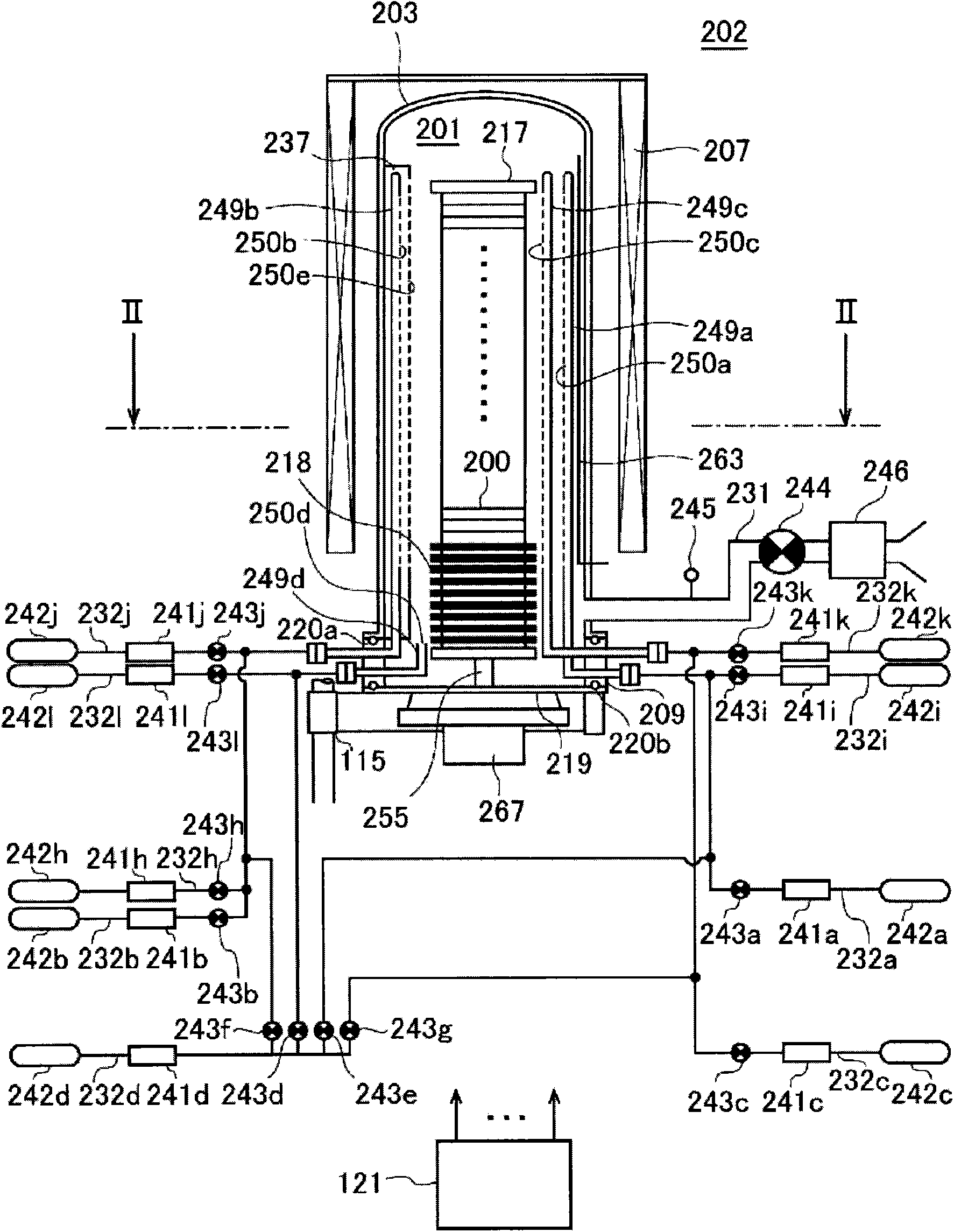
[0246] Although the embodiments of the present disclosure have been described in detail so far. However, the present disclosure is not limited to the aforementioned embodiments or modifications, and various modifications can be made without departing from the spirit of the present disclosure.

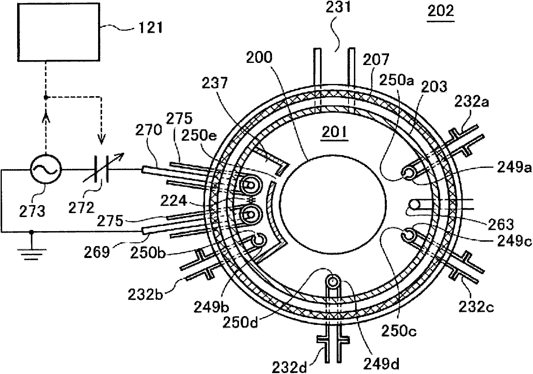
[0247] In the aforementioned embodiment or modification, an example was described in which the SiOC film was formed at a low temperature by supplying a catalytic gas together with a precursor gas or an oxidizing gas, but the configuration of the present disclosure is not limited thereto. For example, without the use of catalytic gas, O 2 A gas or the like as an oxidizing gas can be excited into a plasma state and supplied to the wafer 200 in a state in which its oxidizing ability is enhanced. But in this case, in order to prevent desorption of C from the SiOC film, low high-frequency power is required so that the oxidation reaction proceeds more smoothly.

[0248] In the foregoing emb...


PUM


Abstract

A method for cleaning an interior of a process chamber after performing a process of forming a carbon-containing film on a substrate in the process chamber includes performing a cycle a predetermined number of times. The cycle includes supplying a modifying gas into the process chamber to modify deposits including the carbon-containing film deposited on a surface of a member in the process chamber and supplying an etching gas into the process chamber to remove the modified deposits through a thermochemical reaction.

Description

[0001] Cross References to Related Applications [0002] This application is based on and claims the benefit of priority from Japanese Patent Application No. 2013-137518 filed on June 28, 2013, the entire contents of which are incorporated herein by reference. technical field [0003] The present disclosure relates to cleaning methods, methods of manufacturing semiconductor devices, and substrate processing equipment. Background technique [0004] Fabrication of a semiconductor device includes a process of forming a thin film on a substrate and a process of cleaning the inside of the processing chamber by, for example, supplying an etching gas such as a fluorine-containing gas into the processing chamber after forming the thin film. Through the cleaning process, residual deposits (including the same type of film as the film formed on the substrate) deposited in the processing chamber when forming the thin film on the substrate are removed. [0005] When a thin film formed ...

Claims


Application Information

Patent Timeline
Patent Type & Authority Applications(China)
IPC IPC(8): B08B7/00H01L21/02
CPCC23C16/4405H01L21/02049H01L21/02126
Inventor 野田孝晓野原慎吾广濑义朗
Owner KOKUSA ELECTRIC CO LTD
Why Eureka
Try Eureka