Integrated circuit with backside structure reducing substrate warpage

A technology of integrated circuits and substrates, applied in the field of integrated circuits with backside structures, can solve problems such as difficulty in development

Active Publication Date: 2017-05-10
TAIWAN SEMICON MFG CO LTD
View PDF8 Cites 1 Cited by
  • Summary
  • Abstract
  • Description
  • Claims
  • Application Information

AI Technical Summary

Problems solved by technology

Although substantial increases in density have been achieved within the constraints of two-dimensional layouts, further advances have been difficult to achieve

Method used


Image

  • Integrated circuit with backside structure reducing substrate warpage
  • Integrated circuit with backside structure reducing substrate warpage
  • Integrated circuit with backside structure reducing substrate warpage

Examples


Embodiment Construction

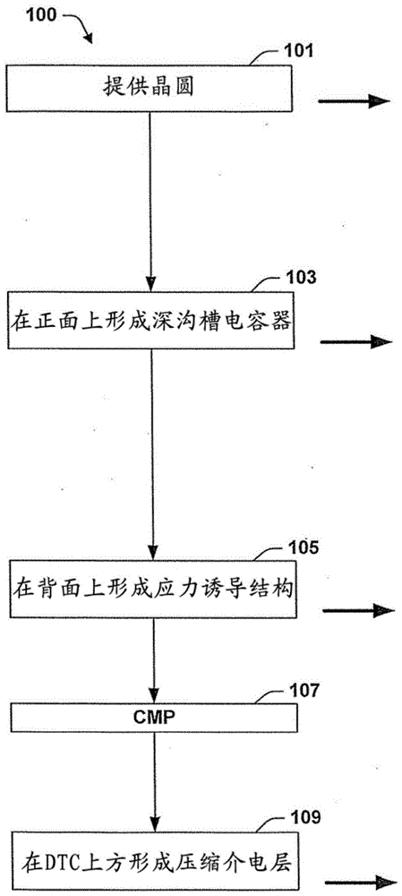
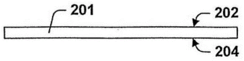
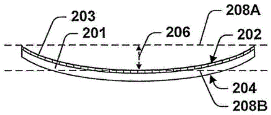
[0043] During the fabrication of integrated circuit devices having deep trench capacitors, the wafer on which the capacitors are formed may become warped. The inventors have found that this bending phenomenon is particularly severe for deep trench capacitors with multiple conductive layers. Bowing can be to the extent that it can adversely affect subsequent processes such as chemical mechanical polishing. Such bowing can be especially problematic for wafers from which 3D-IC devices are formed.

[0044] The inventors solved this problem by forming structures with tensile stress on the backside of the wafer. In some embodiments, these structures are tensile membranes. In some embodiments, these structures include trenches filled with tensile material. Structures located on the backside of the wafer can sufficiently reduce wafer bow to allow further processing. In some embodiments, bowing is further reduced by forming one or more compressive films over the capacitors on the f...


PUM


Abstract

The present invention improves wafer warpage caused by deep trench capacitors through structures formed on the reverse side of the wafer. The structure on the reverse side includes a tensioned membrane. A tension film can be formed in the trenches on the backside of the wafer, which enhances its effect. In some embodiments, wafers are used to form 3D-IC devices. In some embodiments, a 3D-IC device includes high voltage or high power circuitry. The invention also discloses an integrated circuit with a backside structure that reduces substrate warpage.

Description

technical field [0001] The invention relates to the technical field of semiconductors, in particular to an integrated circuit with a backside structure that reduces substrate warpage. Background technique [0002] Since the invention of the integrated circuit, the semiconductor industry is constantly looking for ways to increase the integration of integrated circuit components (transistors, diodes, resistors, capacitors, etc.). In most cases, the increase in density comes from a reduction in feature size, allowing more components to be formed in a given area. Despite these advances, the components have remained in a basic two-dimensional layout. While substantial increases in density have been achieved within the constraints of two-dimensional layouts, further advances have been difficult to achieve. [0003] Three-dimensional integrated circuits (3D ICs) have been created to overcome these limitations. In a 3D IC, two or more semiconductor bodies are formed vertically al...

Claims


Application Information

Patent Timeline
Patent Type & Authority Patents(China)
IPC IPC(8): H01L27/06H01L21/02
CPCH01L2224/32145H01L2224/32225H01L2224/48227H01L2224/73253H01L2224/73265H01L2924/15311H01L2924/3511H01L24/73H01L21/302H01L28/60H01L28/40H01L23/562H10B12/37H10B12/038H01L2924/00012H01L2924/00H01L21/02016H01L21/8221H01L21/02164H01L21/02236H01L21/30625H01L21/3205H01L21/76802H01L21/76877H01L21/78H01L22/20H01L24/83H01L25/0657H01L25/50H01L2224/48091H01L2224/48106H01L2225/0651H01L2225/06548H01L2225/06555H01L2225/06575H01L2225/06586H01L2924/14H01L2924/1436
Inventor 陈志明王嗣裕喻中一
Owner TAIWAN SEMICON MFG CO LTD
Why Eureka
Try Eureka