Wafer bow reduction

a composite wafer and bow technology, applied in the direction of polycrystalline material growth, crystal growth process, chemically reactive gas, etc., to achieve the effect of reducing the bow of the wafer, reducing stress, and improving the robustness of the wafer

Active Publication Date: 2020-07-14
ANVIL SEMICON
View PDF11 Cites 0 Cited by
  • Summary
  • Abstract
  • Description
  • Claims
  • Application Information

AI Technical Summary

Benefits of technology

[0006]The present invention reduces wafer bow by introducing a countermanding compressive stress at the critical place in the composite wafer, i.e. at the Si / SiC interface. There are two motivations for wishing to reduce stress and bow. The first is to improve the robustness of the wafer, because highly stressed wafers break easily. The second is to produce as flat a wafer as possible to facilitate its processing through the various equipment used to realise microelectronic components.
[0007]According to one aspect of the present invention, there is provided a method for reducing bow in a composite wafer comprising a silicon wafer and a silicon carbide layer grown on the silicon wafer. The method comprises applying nitrogen atoms during the epitaxial growth of the silicon carbide epitaxial layer on the silicon wafer so as to generate a compressive stress within the composite wafer. The technique allows the nitrogen atoms to be incorporated into the wafer during the initial epitaxial growth process of the epitaxial layer. This technique generates a compressive stress within the wafer which countermands the bow causing tensile stress within the wafer.
[0014]The application of the nitrogen atoms may generate the compressive stress to countermand a natural tensile stress causing the bow of the composite wafer.
[0018]The application of nitrogen atoms may cause the substantially central part of the composite wafer to be substantially flattened so as to reduce the bow of the composite wafer. This technique enables the overall the wafer to be substantially flattened so that one or more layers can be easily grown on top of the initial heteroepitaxy and to facilitate normal semiconductor device processing steps.

Problems solved by technology

The challenge in producing silicon carbide / silicon, particularly 3-step cubic silicon carbide (3C—SiC) and Si heteroepitaxy, is the tensile stress introduced at the Si / SiC interface due to the lattice miss-match between the two materials and the faster thermal contraction of SiC while cooling down from the typical growth temperature of 1370° C.

Method used


Image

  • Wafer bow reduction
  • Wafer bow reduction
  • Wafer bow reduction

Examples


Embodiment Construction

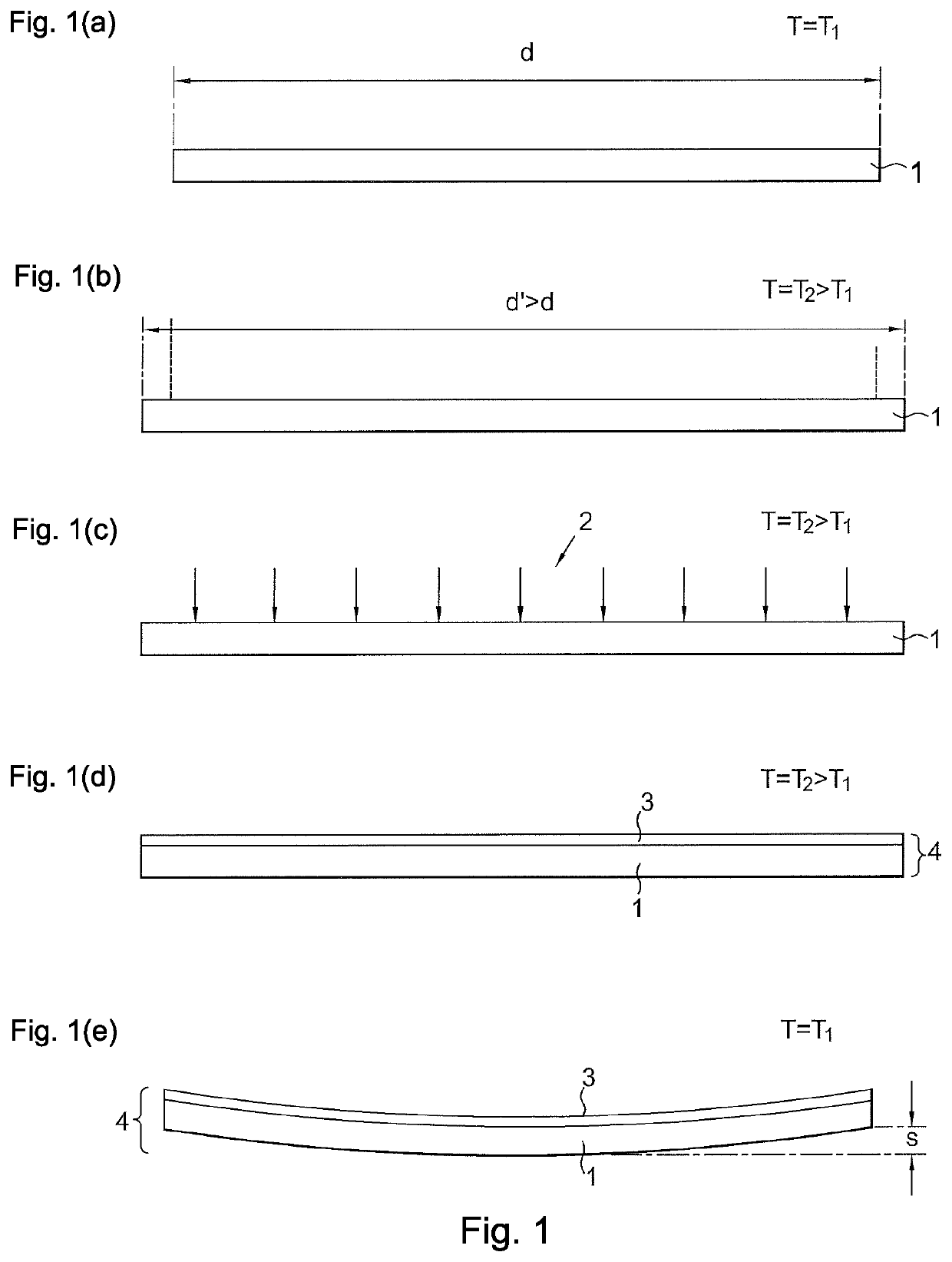
[0043]Before describing embodiments of the present invention, a silicon carbide / silicon heteroepitaxy process will be described with reference to FIGS. 1a to 1e which may be useful for understanding the present invention.

[0044]FIG. 1a shows a monocrystalline silicon wafer 1 at a room temperature (about 25° C.). The silicon wafer 1 serves as a seed wafer on which a layer of three-step cubic silicon carbide (3C—SiC) can be epitaxially grown. The silicon wafer 1 has a diameter, d.

[0045]The silicon wafer 1 is placed in a silicon carbide epitaxial reactor (not shown) and is heated to about 1350° C. As shown (in highly schematic form) in FIG. 1b, the silicon wafer 1 expands when heated. The heated wafer has a diameter, d′, greater than diameter, d, of the wafer at room temperature.

[0046]Referring to FIG. 1c, the heated silicon wafer 1 is exposed to a vapour 2 of silicon and carbon reactive species in a chemical vapour deposition (CVD) process. The vapour 2 adsorbs on the silicon wafer 1 f...


PUM

PropertyMeasurementUnit
heightaaaaaaaaaa
compressive stressaaaaaaaaaa
doping concentrationaaaaaaaaaa

Abstract

We describe a method for reducing bow in a composite wafer comprising a silicon wafer and a silicon carbide layer grown on the silicon wafer. The method includes applying nitrogen atoms during the growth process of the silicon carbide layer on the silicon wafer so as to generate a compressive stress within the composite wafer.

Description

RELATED APPLICATIONS[0001]This application is a Continuation-in-Part of International Patent Application No. PCT / GB2015 / 054159, filed on 23 Dec. 2016; which claims priority from 1500558.0, filed 14 Jan. 2015, the entirety of both of which are incorporated herein by reference.FIELD OF THE INVENTION[0002]This invention relates to bow reduction in a composite wafer, particularly but not exclusively, in a silicon carbide (SiC) based composite wafer.BACKGROUND TO THE INVENTION[0003]The challenge in producing silicon carbide / silicon, particularly 3-step cubic silicon carbide (3C—SiC) and Si heteroepitaxy, is the tensile stress introduced at the Si / SiC interface due to the lattice miss-match between the two materials and the faster thermal contraction of SiC while cooling down from the typical growth temperature of 1370° C.[0004]It has already been demonstrated that dividing the surface of the wafer into sub-die of the order of 2.5 mm per side with thin lines of polycrystalline SiC is bene...

Claims


Application Information

Patent Timeline
Patent Type & Authority Patents(United States)
IPC IPC(8): C30B25/18H01L29/34C30B25/02C30B29/06C30B29/36H01L21/02H01L29/739H01L29/16H01L29/66H01L29/08H01L29/861H01L29/78
CPCH01L29/0834C30B29/36H01L29/66068H01L29/1608H01L21/02381H01L21/02529C30B25/02H01L29/34H01L21/02694C30B25/18H01L21/0262H01L29/7395H01L21/02378H01L21/02576C30B29/06H01L29/7802H01L29/861H01L21/0257H01L21/20
Inventor WARD, PETER
Owner ANVIL SEMICON
Why Eureka
Try Eureka