
Integrated wafer bow measurements

A wafer and warpage technology, applied in the field of integrated wafer warpage measurement, can solve the problems of not being able to provide warpage compensation in real time, not suitable for process control, not suitable for real-time measurement, etc.

Pending Publication Date: 2021-08-31
LAM RES CORP
View PDF1 Cites 0 Cited by
  • Summary
  • Abstract
  • Description
  • Claims
  • Application Information

AI Technical Summary

Problems solved by technology

[0012] Current stand-alone technologies are either limited by TpT (wafer to point-by-point measurement) or have <300 micron measurement range, making them unsuitable for process control
Also, stand-alone systems are not designed to measure hot wafers and are therefore not suitable for real-time measurements
For example, in some cases wafer warp compensation can be performed by depositing a film on the backside of a warped wafer using a deposition tool, but this does not provide sufficient warp compensation in real-time in high-volume manufacturing

Method used


Image

  • Integrated wafer bow measurements
  • Integrated wafer bow measurements
  • Integrated wafer bow measurements

Examples


Embodiment Construction

[0047] The following description includes systems, methods, techniques, instruction sequences, and computing machine program products that embody illustrative embodiments of the invention. In the following description, for purposes of explanation, numerous specific details are set forth in order to provide a thorough understanding of example embodiments. It will be apparent, however, to one skilled in the art that the present embodiment may be practiced without these specific details.

[0048] Portions of the disclosure of this patent document contain material that is protected by copyright. The copyright owner has no objection to the facsimile reproduction by anyone of the patent document or the patent disclosure as it appears in the Patent and Trademark Office patent files or records, but reserves all copyright in any other respects. The following notice applies to any data as described below and in the drawings forming part of this document: Copyright LAM Research Corporat...


PUM


Abstract

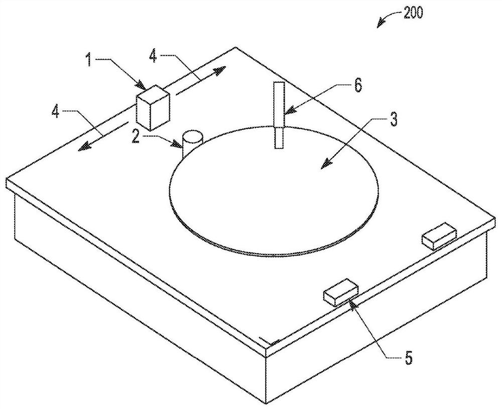
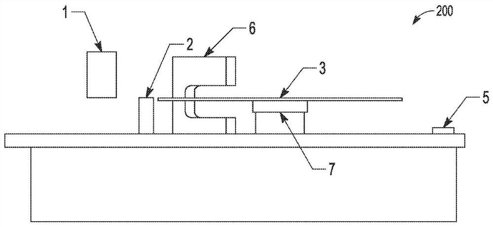
In some examples, a wafer bow measurement system comprises a measurement unit including: a wafer support assembly to impart rotational movement to a measured wafer supported in the measurement unit; an optical sensor; a calibration standard to calibrate the optical sensor; a linear stage actuator to impart linear direction of movement to the optical sensor; a wafer centering sensor to determine a centering of the measured wafer supported in the measurement unit; and a wafer alignment sensor to determine an alignment of the measured wafer supported in the measurement unit.

Description

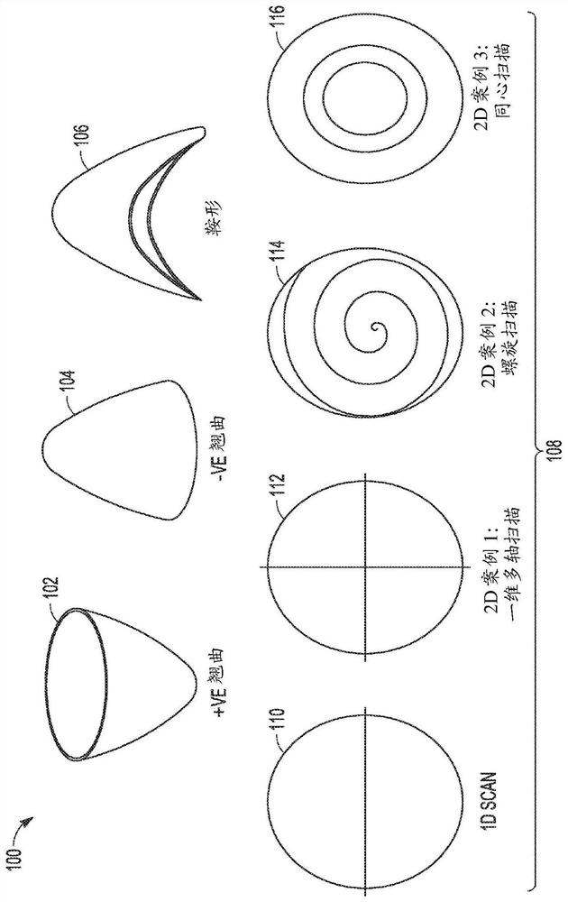
[0001] priority claim [0002] This application claims priority to U.S. Patent Application No. 62 / 796,963, filed January 25, 2019, by Arora et al., entitled "Integrated WaferBow Measurements," which is hereby incorporated by reference in its entirety. technical field [0003] The subject matter disclosed herein relates to devices used in semiconductor and related industries. More specifically, the present disclosure relates to integrated wafer warp measurement, and in one example, wafer warp measurement using optical sensors. Background technique [0004] The background description provided herein is for the purpose of generally presenting the context of the disclosure. The work of the presently named inventors is neither expressly nor impliedly admitted to be prior art to the present disclosure to the extent that it is described in this Background section and in aspects of the specification that cannot be determined to be prior art at the time of filing. technology. [0...

Claims


Application Information

Patent Timeline
IPC IPC(8): H01L21/66G01B11/06H01L21/67
CPCH01L21/67288H01L21/6719H01L21/67259G01B11/06G01B2210/56H01L22/12G01N21/9505H01L21/681
Inventor 拉詹·阿罗拉迈克尔·苏扎韦恩·邓亚辛·卡布兹冯烨
Owner LAM RES CORP
Learn More