A label for attaching satellite surface and its manufacturing method
A manufacturing method and label technology, applied in chemical instruments and methods, ion implantation plating, coating, etc., can solve the problems of satellite thermal control design and construction difficulty of thermal control components, and achieve the effect of good space environment adaptability
- Summary
- Abstract
- Description
- Claims
- Application Information
AI Technical Summary
Problems solved by technology
Method used
Image
Examples
example 1
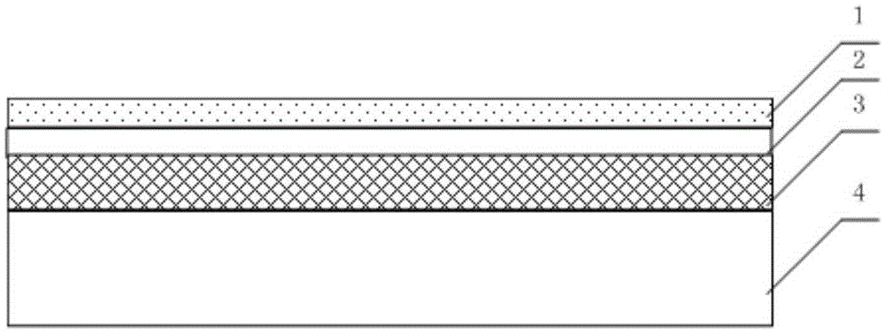
[0030] A label for mounting satellite surfaces, the label is mainly composed of a film base, a paint film layer, a transparent emissivity adjustment layer and a transparent antistatic layer; wherein the film base is polyimide, and its thickness is 50 μm; The paint film (paint) layer is a silicone resin-based paint with a thickness of 30 μm; the transparent emissivity adjustment layer is a silicon dioxide film with a thickness of 200 nm; the transparent antistatic layer is an indium tin oxide film, Its thickness is 100 nm.
example 2
[0032] A label for mounting satellite surfaces, the label is mainly composed of a film base, a paint film layer, a transparent emissivity adjustment layer and a transparent antistatic layer; wherein the film base is polyimide, and its thickness is 75 μm; The paint film (paint) layer is a silicone resin-based paint with a thickness of 50 μm; the transparent emissivity adjustment layer is a titanium dioxide film with a thickness of 300 nm; the transparent antistatic layer is an indium tin oxide film with a thickness of 50 μm. 200nm.
example 3
[0034] A label for mounting a satellite surface, the label is mainly composed of a film base, a paint film layer, a transparent emissivity adjustment layer and a transparent antistatic layer; wherein the film base is F46, and its thickness is 50 μm; the paint The film (paint) layer is a silicone resin-based paint with a thickness of 70 μm; the transparent emissivity adjustment layer is a silicon dioxide film with a thickness of 400 nm; the transparent antistatic layer is a zinc oxide film with a thickness of 50 nm .
[0035] A method for making a label for mounting a satellite surface, the specific steps are:
[0036] Step 1, printing a paint film layer on the film substrate by screen printing, and the paint film layer is used to display the pattern of the label;
[0037] Step 2, preparing a transparent emissivity adjusting layer to adjust the emissivity of the label by depositing three times by magnetron sputtering on the paint film layer;
[0038] Step 3, preparing a trans...
PUM
| Property | Measurement | Unit |
|---|---|---|
| thickness | aaaaa | aaaaa |
| thickness | aaaaa | aaaaa |
| thickness | aaaaa | aaaaa |
Abstract
Description
Claims
Application Information
