A method for measuring electron beam spot size of scanning electron microscope

An electron microscope and electron beam technology, applied in the field of electronics, can solve the problems of imprecise imaging measurement error, complex production process, measurement error and troublesome operation process, and achieve the effect of improving contrast, simple operation and strong practicability

Inactive Publication Date: 2017-08-11
UNIV OF ELECTRONICS SCI & TECH OF CHINA
View PDF13 Cites 0 Cited by
  • Summary
  • Abstract
  • Description
  • Claims
  • Application Information

AI Technical Summary

Problems solved by technology

Accurate measurement of electron beam current value of scanning electron microscope can be realized by Faraday cup. The current method for measuring electron beam spot size is mainly realized by electron beam exposure glue or by measuring electron beam current. In the measurement, the electron beam exposure glue is difficult to apply due to the shortcomings of complex film production process, cumbersome development and fixing process, inaccurate imaging and large measurement error; and the method of measuring current to measure the beam spot is prone to measurement due to problems such as electron beam scattering. errors, and the need to use a microcurrent meter to measure the current, and at the same time, the sample chamber of the scanning electron microscope needs to be modified, which brings a lot of measurement errors and troubles in the operation process

Method used


Image

  • A method for measuring electron beam spot size of scanning electron microscope
  • A method for measuring electron beam spot size of scanning electron microscope
  • A method for measuring electron beam spot size of scanning electron microscope

Examples


Embodiment Construction

[0020] In order to make the technical means, creative features, goals and effects achieved by the present invention easy to understand, the present invention will be further described below in conjunction with specific diagrams.

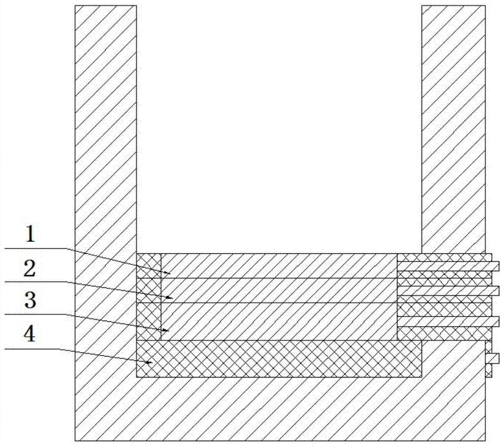
[0021] refer to figure 2 The schematic diagram of the structure of the Faraday cup is shown. The Faraday cup with a grid is designed and manufactured. The purpose of adding the grid is to intercept the secondary electrons generated by the electron beam hitting the inner plate of the Faraday cup, thereby effectively enhancing the force at the edge of the blade sample. contrast.

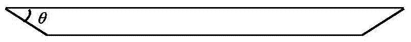
[0022] refer to image 3 The metal flake shown is a metal blade. The blade sample has a wide top and a bottom narrow section. At the same time, it is necessary to ensure that the surface smoothness and finish of the blade sample are as high as possible.

[0023] refer to Figure 4 The measurement device and sample placement diagram shown in the diagram place the Faraday ...


PUM


Abstract

The invention relates to a method for measuring the size of an electron beam spot of a scanning electron microscope, which relates to the field of electronic technology, and in particular to a measuring method for measuring the size of an electron beam spot of a scanning electron microscope. First, the metal blade placed on the mouth of the Faraday cup is irradiated by a scanning electron microscope to obtain a clear image of the metal blade; then part of the image of the edge of the knife is intercepted, and the RGB value of the intercepted image is obtained by image data processing software to obtain R, G, B three Then calculate the average value of these three matrices to obtain an average matrix; sum each column of the average matrix to obtain a one-dimensional matrix, and draw a two-dimensional curve according to the values ​​of each unit of the one-dimensional matrix , the width of the rising edge of the curve is the beam spot diameter of the electron beam, so as to achieve the purpose of the invention. Therefore, it has the effects of simple operation, high precision and strong practicability.

Description

technical field [0001] The invention relates to the field of electronic technology, in particular to a measuring method for measuring the electron beam spot size of a scanning electron microscope. Background technique [0002] In the related application of high-resolution scanning electron microscope, the parameters of scanning electron microscope electron beam are of great significance to characterize the working performance of scanning electron microscope, especially the current size and beam spot size of electron beam. The current value of the electron beam will affect the brightness of the electron beam, and the beam spot size of the electron beam will determine the imaging resolution of the scanning electron microscope. Therefore, it is very necessary to accurately measure the beam spot size of the electron beam. Accurate measurement of electron beam current value of scanning electron microscope can be realized by Faraday cup. The current method for measuring electron ...

Claims


Application Information

Patent Timeline
Patent Type & Authority Patents(China)
IPC IPC(8): G01B7/00
Inventor 胡旻丁德成刘盛纲
Owner UNIV OF ELECTRONICS SCI & TECH OF CHINA
Why Eureka
Try Eureka