Phase inverter, drive circuit and display panel

A technology of inverters and capacitors, applied in logic circuits, instruments, electrical components, etc., can solve problems such as unstable output signals and achieve good display effects

Active Publication Date: 2015-01-07
WUHAN TIANMA MICRO ELECTRONICS CO LTD +1
View PDF8 Cites 19 Cited by
  • Summary
  • Abstract
  • Description
  • Claims
  • Application Information

AI Technical Summary

Problems solved by technology

[0005] In view of this, an embodiment of the present invention provides an inverter, a driving circuit, and a display panel to solve the problem in the prior art that the output signal of the inverter is unstable when the first clock signal changes from a low level to a high level. technical problem

Method used


Image

  • Phase inverter, drive circuit and display panel
  • Phase inverter, drive circuit and display panel
  • Phase inverter, drive circuit and display panel

Examples


Embodiment 1

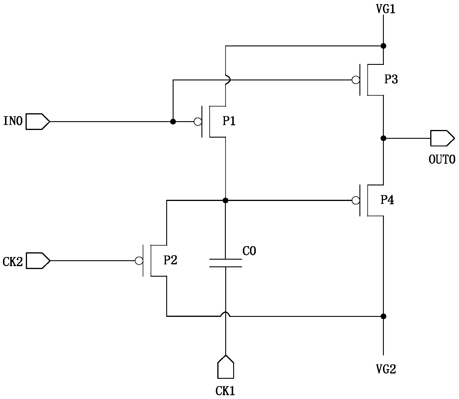
[0032] Embodiment 1 of the present invention provides an inverter, and the inverter includes: a first transistor, a second transistor, a third transistor, a fourth transistor, a fifth transistor, a first capacitor, and a second capacitor; The gate of a transistor is electrically connected to the start signal input end for receiving the start signal, the source is electrically connected to the first level signal input end for receiving the first level signal, and the drain is electrically connected to the second transistor The source of the fifth transistor and the gate of the fifth transistor; the drain of the second transistor is electrically connected to the first clock signal input terminal for receiving the first clock signal through the first capacitor; the third transistor The gate of the gate is electrically connected to the second clock signal input terminal for receiving the second clock signal, the source is electrically connected to the drain of the second transistor...

Embodiment 2

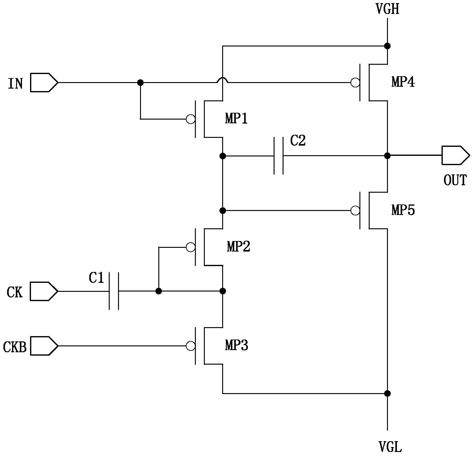
[0039] Figure 2a It is a circuit diagram of an inverter provided in Embodiment 2 of the present invention. see Figure 2a , the inverter according to Embodiment 2 of the present invention includes: a first transistor MP1, a second transistor MP2, a third transistor MP3, a fourth transistor MP4, a fifth transistor MP5, a first capacitor C1, and a second capacitor C2; The gate of a transistor MP1 is electrically connected to the initial signal input terminal IN for receiving the initial signal, the source is electrically connected to the first level signal input terminal VGH for receiving the first level signal, and the drain is electrically connected to the The source of the second transistor MP2 and the gate of the fifth transistor MP5; the gate of the second transistor MP2 is electrically connected to its drain, and the drain is used to receive the first clock signal through the first capacitor C1 The first clock signal input terminal CK is electrically connected; the gate...

Embodiment 3

[0053] this invention Figure 5a It is a circuit diagram of an inverter provided in Embodiment 3 of the present invention. see Figure 5a , the inverter according to Embodiment 3 of the present invention includes: a first transistor MP1, a second transistor MP2, a third transistor MP3, a fourth transistor MP4, a fifth transistor MP5, a first capacitor C1, and a second capacitor C2; The gate of a transistor MP1 is electrically connected to the initial signal input terminal IN for receiving the initial signal, the source is electrically connected to the first level signal input terminal VGH for receiving the first level signal, and the drain is electrically connected to the The source of the second transistor MP2 and the gate of the fifth transistor MP5; the gate of the second transistor MP2 is electrically connected to the second level signal input terminal VGLS, and the drain passes through the first capacitor C1 It is electrically connected to the first clock signal input t...


PUM


Abstract

The invention discloses a phase inverter, a drive circuit and a display panel. The phase inverter comprises a first transistor, a second transistor, a third transistor, a fourth transistor, a fifth transistor, a first capacitor and a second capacitor. According to the technical scheme, the second transistor is controlled through the grid electrode of the second transistor to be prevented from being switched on reversely, and the electric potential of the grid electrode of the fifth transistor is maintained through the second capacitor. When a first clock signal is changed into a low level from a high level (correspondingly, the first transistor, the second transistor, the third transistor, the fourth transistor and the fifth transistor are all NMOS transistors) or changed into a high level from a low level (correspondingly, the first transistor, the second transistor, the third transistor, the fourth transistor and the fifth transistor are all PMOS transistors), the electric potential of the grid electrode of the fifth transistor can be kept stable. In this way, the output signals of the phase inverter can be free of influences of changes of the first clock signal, the phase inverter can generate stable output signals, and then the display panel with the phase inverter can achieve a better display effect.

Description

technical field [0001] The invention relates to the field of display technology, in particular to an inverter, a driving circuit and a display panel. Background technique [0002] The inverter has a reverse effect on the start signal input to it. It can also be said that the output signal of the inverter and the start signal are mutually inverse signals. With the development of electronic technology, the application of the inverter is becoming more and more extensive. For example, the inverter can be applied to the emission drive circuit of the organic light-emitting display device, and provides a corresponding potential for the pixel compensation circuit electrically connected to the emission drive circuit. Make the pixel compensation circuit complete node initialization, threshold compensation and data writing, etc. [0003] Figure 1a is a circuit diagram of a prior art inverter. Such as Figure 1a As shown, the inverter includes a first transistor P1, a second transist...

Claims


Application Information

Patent Timeline
Patent Type & Authority Applications(China)
IPC IPC(8): G09G3/32G09G3/3208
CPCG09G3/3266G09G2310/0291H03K19/00315H03K19/0944Y02B70/10H02M1/0054
Inventor 钱栋李玥张通王志良罗丽媛
Owner WUHAN TIANMA MICRO ELECTRONICS CO LTD
Why Eureka
Try Eureka