LED chip packaging method and LED packaging structure using same

A technology of LED chip and packaging method, which is applied in the direction of electrical components, circuits, semiconductor devices, etc., can solve the problems of complex process, large equipment investment, low production efficiency, etc., and achieve the effect of simple process and uniform light emission

Active Publication Date: 2015-01-07
LEEDARSON IOT TECH INC
View PDF6 Cites 3 Cited by
  • Summary
  • Abstract
  • Description
  • Claims
  • Application Information

AI Technical Summary

Problems solved by technology

This process has the disadvantages of requiring a large amount of equipment investment, complex process, and low production efficiency.

Method used


Image

  • LED chip packaging method and LED packaging structure using same
  • LED chip packaging method and LED packaging structure using same
  • LED chip packaging method and LED packaging structure using same

Examples


Embodiment Construction

[0022] The present invention will be further described in detail below in conjunction with the accompanying drawings and specific embodiments.

[0023] Please refer to Figure 1A to Figure 1E , Figures 1A to 1E is a schematic diagram of the steps of the first embodiment of the LED chip packaging method of the present invention, and the LED chip packaging method of the first embodiment of the present invention includes the following steps:

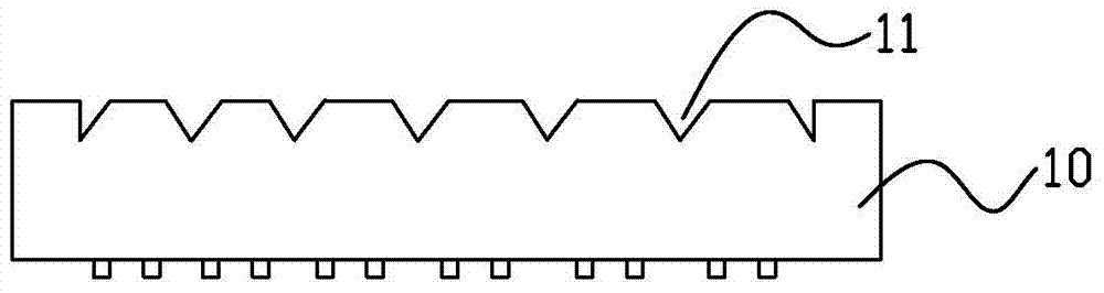
[0024] First, please refer to Figure 1A , Figure 1B , making an epitaxial wafer 10 of the LED chip, cutting and forming a groove 11 on the top of the epitaxial wafer 10;

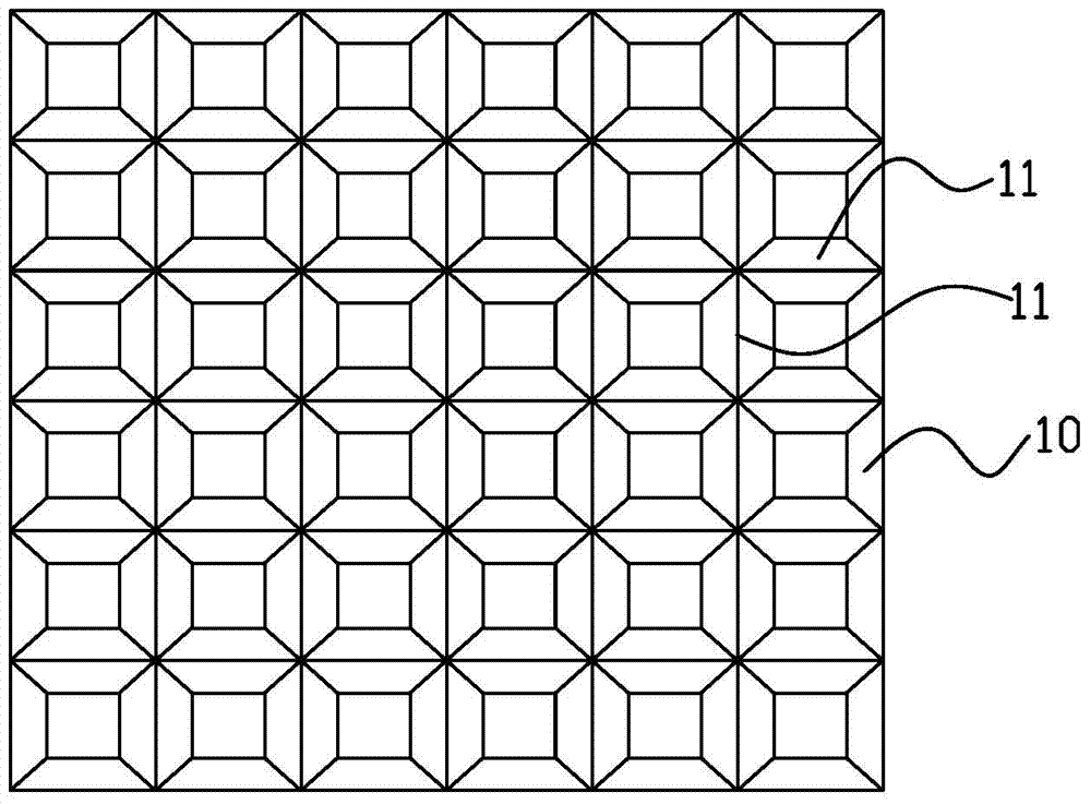
[0025] These grooves 11 are V-shaped structures, these grooves 11 form a grid shape on the top of the epitaxial wafer 10, and each grid corresponds to each LED chip to be formed.

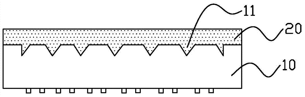
[0026] Second, please refer to Figure 1C , the top of the epitaxial wafer 10 is provided with a thin film 20;

[0027] Phosphor powder is mixed in the film 20, and the phosphor powder ...


PUM


Abstract

The invention provides an LED chip packaging method. The method comprises the following steps that an epitaxial wafer of an LED chip is made, and the top of the epitaxial wafer is cut to form a groove; a thin film is arranged on the top of the epitaxial wafer; the thin film and the epitaxial wafer are cut along the groove to form multiple LED chips, and a chamfer is formed on the top of each cut LED chip; the cut LED chips are heated, so that the thin film is molten and wrapped on the LED chips, and a packaging layer is formed when curing is conducted after the thin film is cooled. The invention further provides an LED packaging structure using the LED chip packaging method. The LED chip packaging method and the LED packaging structure using the LED chip packaging method have the advantage that the process is simple.

Description

technical field [0001] The invention relates to the technical field of LED packaging, in particular to an LED chip packaging method and an LED packaging structure using the packaging method. Background technique [0002] At present, there are many packaging methods for LEDs. A common packaging method in the industry is to complete the two steps of first soldering the chip and then coating the phosphor. For example, the invention patent application with the application number 201110350640.1 published on July 11, 2012 disclosed a wafer-level LED lens packaging structure and method. The wafer-level LED lens packaging method includes the following steps: A. Make an insulating layer on the insulating layer, and then deposit a metal conductive layer array on the insulating layer; B, make a dam array on the wafer; C, form bump solder balls on the conductive layer and the LED chip; D, pass the LED chip through the inverted The soldering process welds the corresponding metal conduct...

Claims


Application Information

Patent Timeline
Patent Type & Authority Applications(China)
IPC IPC(8): H01L33/58H01L33/48
CPCH01L33/005H01L33/48H01L33/58H01L2933/0033H01L2933/0058
Inventor 张晓娟郭伟杰马志超李江淮
Owner LEEDARSON IOT TECH INC
Why Eureka
Try Eureka