Fabrication method of cascaded stacked nanowire MOS transistors

A MOS transistor, stacking nanowire technology, applied in semiconductor/solid-state device manufacturing, semiconductor devices, electrical components, etc., can solve problems such as increasing process costs, and achieve the effect of increasing the total effective conductive cross-sectional area and driving current.

Active Publication Date: 2018-07-27
INST OF MICROELECTRONICS CHINESE ACAD OF SCI
View PDF2 Cites 0 Cited by
  • Summary
  • Abstract
  • Description
  • Claims
  • Application Information

AI Technical Summary

Problems solved by technology

This method is severely limited by the quality of the epitaxial thin layer, which greatly increases the process cost

Method used


Image

  • Fabrication method of cascaded stacked nanowire MOS transistors
  • Fabrication method of cascaded stacked nanowire MOS transistors
  • Fabrication method of cascaded stacked nanowire MOS transistors

Examples


Embodiment Construction

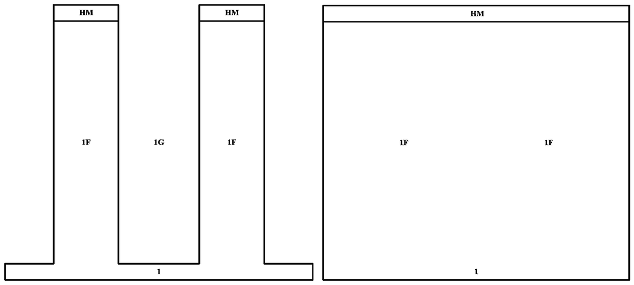
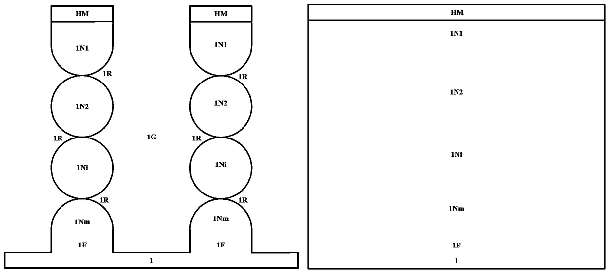
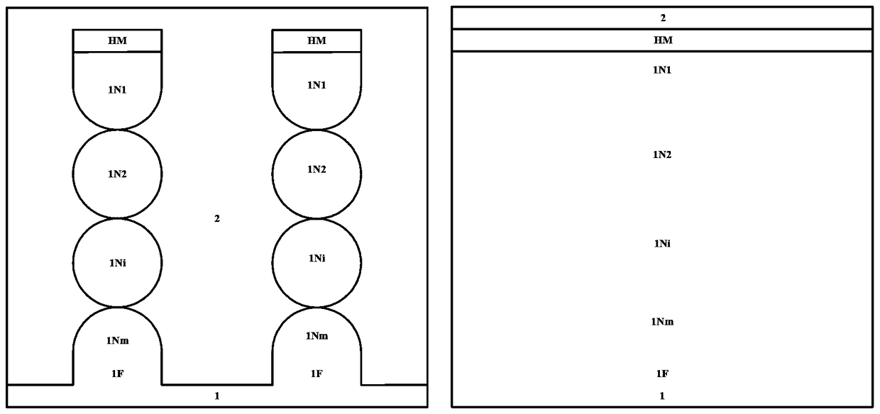
[0025] The features and technical effects of the technical solution of the present invention will be described in detail below with reference to the accompanying drawings and in conjunction with schematic embodiments, and a stacked nanowire MOS transistor and a manufacturing method thereof are disclosed that sufficiently increase the effective width of the conductive channel to increase the driving current. It should be pointed out that similar reference numerals represent similar structures, and the terms "first", "second", "upper", "lower" and the like used in this application can be used to modify various device structures or manufacturing processes . These modifications do not imply spatial, sequential or hierarchical relationships of the modified device structures or fabrication processes unless specifically stated.

[0026] Figure 9 Shown is a schematic perspective view of a stacked nanowire MOS transistor manufactured in accordance with the present invention, wherein ...


PUM


Abstract

The invention discloses a stacked nanowire MOS transistor and a manufacturing method thereof, comprising: a plurality of nanowire stacks extending along a first direction on a substrate; a plurality of gate stacks extending along a second direction and spanning each Nanowire stack; a plurality of source and drain regions, located on both sides of each gate stack along the second direction; a plurality of channel regions, composed of nanowire stacks located between the plurality of source and drain regions; wherein the plurality of nanowire stacks A stack of multiple nanowires connected in cascade. According to the stacked nanowire MOS transistor and the manufacturing method thereof of the present invention, a cascaded nanowire stack with good quality is formed by multiple times of etching back, laterally etching the trench and filling it, and the conductive trench is fully enlarged at a lower cost The effective width of the track is increased, and the total effective conductive cross-sectional area is increased, thereby increasing the driving current.

Description

technical field [0001] The invention relates to a method for manufacturing a semiconductor device, in particular to a novel method for manufacturing a cascaded stacked nanowire MOS transistor. Background technique [0002] In the current sub-20nm technology, the three-dimensional multi-gate device (FinFET or Tri-gate) is the main device structure, which enhances the gate control ability and suppresses leakage and short channel effects. [0003] For example, compared with traditional single-gate bulk Si or SOI MOSFETs, MOSFETs with double-gate SOI structures can suppress short-channel effects (SCE) and drain-induced barrier lowering (DIBL) effects, have lower junction capacitance, and can To achieve light channel doping, the threshold voltage can be adjusted by setting the work function of the metal gate, which can obtain about 2 times the driving current and reduce the requirements for the effective gate oxide thickness (EOT). Compared with the double-gate device, the gate ...

Claims


Application Information

Patent Timeline
Patent Type & Authority Patents(China)
IPC IPC(8): H01L21/336H01L21/28H01L29/78H01L29/10H01L29/423
CPCH01L29/0673H01L29/66439H01L29/78696H01L29/66545H01L29/66772H01L29/78654H01L29/7848H01L29/42384H01L29/66795
Inventor 殷华湘马小龙徐唯佳徐秋霞朱慧珑
Owner INST OF MICROELECTRONICS CHINESE ACAD OF SCI
Why Eureka
Try Eureka