Method for manufacturing high-power high-reflectance COB substrate and light source

A technology with high reflectivity and manufacturing method, applied in the field of light sources, can solve the problems of LED light energy waste, low luminous efficiency of COB light source, light energy waste, etc. Effect

Inactive Publication Date: 2015-01-14
SHENZHEN ZHIJIN ELECTRONICS
View PDF4 Cites 5 Cited by
  • Summary
  • Abstract
  • Description
  • Claims
  • Application Information

AI Technical Summary

Problems solved by technology

[0002] Traditionally produced COB light sources have low luminous efficiency, and the light energy of LEDs is wasted in large quantities
The existing manufacturing method is generally to form a reflective cup structure in the crystal-bonding area of ​​the LED chip to concentrate the light emitting angle of the LED chip, thereby improving the light efficiency, but there is still a lot of waste of light energy in this way

Method used


Image

  • Method for manufacturing high-power high-reflectance COB substrate and light source
  • Method for manufacturing high-power high-reflectance COB substrate and light source

Examples


Embodiment Construction

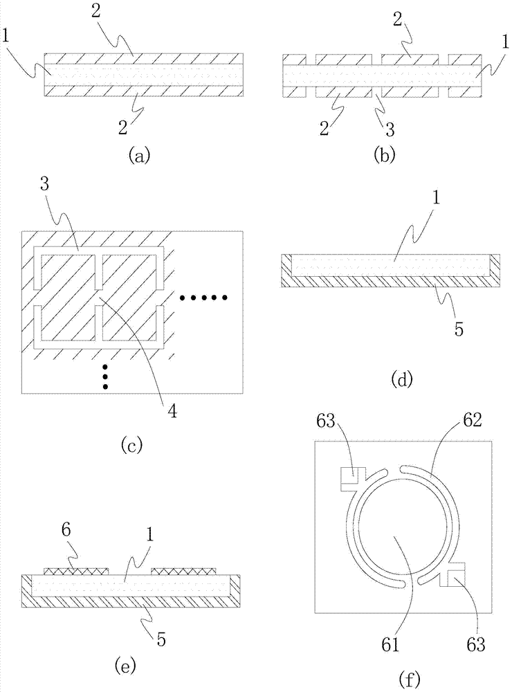
[0032] The present invention will be described in further detail below in conjunction with the accompanying drawings and specific embodiments.

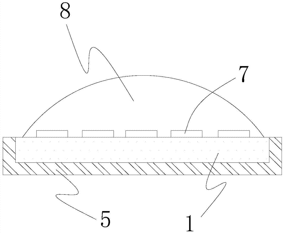
[0033] like figure 1 As shown, the manufacturing method of the high-power high-reflectivity COB substrate of the present invention comprises the following steps:

[0034] (1) Provide a transparent substrate plate 1; transparent substrates such as transparent glass, transparent ceramics or sapphire can be selected, and the light transmittance is high, so that this scheme can be implemented more effectively; the thickness can be selected according to product requirements, and the average thickness is 0.4-4mm. Can.

[0035] (2) A photosensitive film 2 is formed on both sides of the transparent base plate 1; the photosensitive film 2 may be printed or bonded with a photosensitive dry film, and the photosensitive dry film is also a kind of photosensitive film. like figure 1 (a), where figure 1 (a) shows a schematic view of the side vie...


PUM


Abstract

The invention provides a method for manufacturing a high-power high-reflectance COB substrate and light source. The method comprises the following steps that a transparent substrate body is provided; light sensitive films are formed in the two sides of the transparent substrate body; exposure developing is carried out on the light sensitive films on the two sides of the transparent substrate body, and the appearance frame lines of a product on the transparent substrate body are exposed out; the penetrating step is carried out on the appearance frame lines of the product on the transparent substrate body; the light sensitive films are removed; mirror face reflecting layers are formed on the bottom face and the side faces of the transparent substrate body after the light sensitive films are removed; a circuit layer is printed and sintered on the front face of the transparent substrate body after the light sensitive films are removed and a crystal solidification area is arranged on the front face of the transparent substrate body; a weld line area and an electrode are formed on the circuit layer; insulation oil is printed on the other parts, except for the crystal solidification area, the weld line area and the electrode, of the front face of the transparent substrate body. The method for manufacturing the high-power high-reflectance COB substrate and light source can greatly improve the reflecting capacity of the COB substrate or light source, light efficiency is improved, and energy conservation and environment protection are achieved.

Description

technical field [0001] The invention relates to the field of light sources, in particular to a method for manufacturing a COB substrate and a light source. Background technique [0002] Traditional COB light sources have low luminous efficiency, and the light energy of LEDs is wasted in large quantities. The existing manufacturing method is generally to form a reflective cup structure in the die-bonding area of ​​the LED chip to concentrate the light emitting angle of the LED chip, thereby improving the light efficiency, but there is still a lot of waste of light energy in this way. Contents of the invention [0003] In view of the above-mentioned deficiencies in the prior art, the technical problem to be solved by the present invention is to provide a method for manufacturing a COB substrate that can improve the light reflectance of a COB light source and reduce energy waste. [0004] In order to solve the above-mentioned technical problems, the technical solution adopte...

Claims


Application Information

Patent Timeline
Patent Type & Authority Applications(China)
IPC IPC(8): H01L33/48H01L33/60
CPCH01L33/48H01L33/005H01L33/60H01L2933/0033H01L2933/0058
Inventor 康孝恒
Owner SHENZHEN ZHIJIN ELECTRONICS
Why Eureka
Try Eureka