
Memory access method and device for a message-based memory module

A message-based memory and memory module technology, applied in static memory, instrumentation, error detection/correction, etc., can solve problems such as power loss and lack of flexibility, and achieve low power consumption

Active Publication Date: 2017-08-04
HUAWEI TECH CO LTD +1
View PDF5 Cites 0 Cited by
  • Summary
  • Abstract
  • Description
  • Claims
  • Application Information

AI Technical Summary

Problems solved by technology

Chipkill technology achieves high reliability through wider MC bit width and larger granularity data encoding, but this technology can only be used in 4-bit wide DRAM chips in theory, lacks flexibility, and has too large granularity The data encoding causes the data it reads each time is much larger than the actual memory access request data, causing a lot of unnecessary power loss

Method used


Image

  • Memory access method and device for a message-based memory module
  • Memory access method and device for a message-based memory module
  • Memory access method and device for a message-based memory module

Examples


Embodiment 1

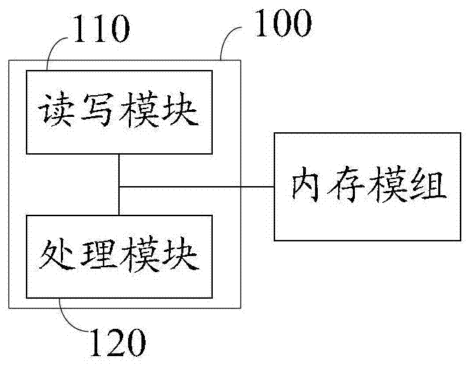
[0029] Please refer to figure 1 , an embodiment of the present invention provides a memory access device for a message-based memory module. The device can be deployed in a peripheral control circuit of a memory module, or in a memory controller; the memory controller can be integrated in a central processing unit (Central Processing Unit, CPU) or integrated on a computer motherboard.

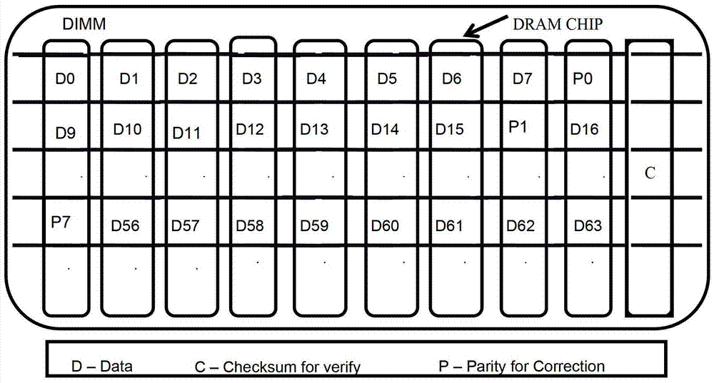
[0030] The memory module may specifically be a DIMM, and the DIMM includes multiple DRAMs. In this paper, it is assumed that the bit width of DRAM is N bits, N is equal to the nth power of 2, and n is a positive integer; the burst length (Burst Length, BL) of DRAM is Q, and Q is a positive integer, preferably Q is equal to several times of 2 Square, for example, it is equal to 4 or 8; assuming that DIMM includes (M+2) blocks of DRAM, (M×N) is the bit width of the entire memory module, because the bit width (M×N) of a computer memory module is generally 2 A number of powers, such as usually 32 ...

Embodiment 2

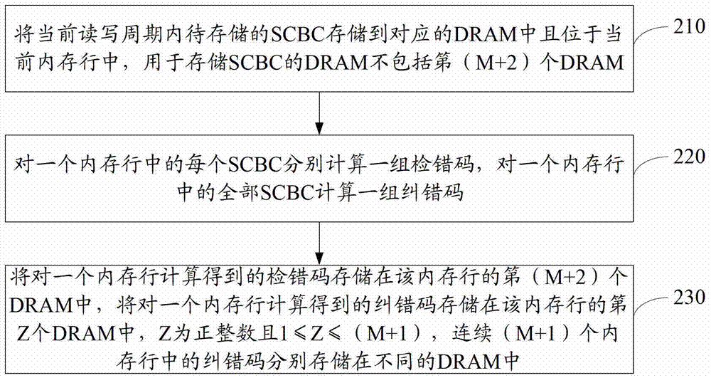
[0065] Please refer to image 3 , the embodiment of the present invention also provides a memory access method of a message-based memory module. The method is executed by a peripheral control circuit or memory controller of the memory module, specifically the memory access device as described in Embodiment 1 deployed in the peripheral control circuit or memory controller. The memory module includes (M+2) block dynamic random access memory (DRAM), M is equal to the m power of 2, and m is a positive integer; The data is called single-chip burst cluster SCBC, and the collection of data stored in all DRAMs that can be accessed in the same read and write cycle forms a memory row.

[0066] The methods include:

[0067] 210. Store the SCBC to be stored in the current read-write cycle into the corresponding DRAM and locate it in the current memory row, and the DRAM used to store the SCBC does not include the (M+2)th DRAM;

[0068] 220. Calculate a set of error detection codes for e...

Embodiment 3

[0080] The embodiment of the present invention also provides a memory control system.

[0081] In one embodiment, as Figure 4a As shown, the system includes a message memory module 310, and the memory module 310 includes a peripheral control circuit 3101 and (M+2) block DRAM 3102;

[0082] Among them, M is equal to the m power of 2, and m is a positive integer; the data stored in each DRAM that can be accessed within one read and write cycle is called single-chip burst cluster SCBC, and the data stored in all DRAMs can be stored in the same The collection of data accessed during a read / write cycle forms a memory row. The memory controller can be integrated on the main board of the computer or in the CPU of the computer.

[0083] The peripheral control circuit performs the following steps:

[0084]The SCBC to be stored in the current read-write cycle is stored in the corresponding DRAM and is located in the current memory row, and the DRAM used to store the SCBC does not in...


PUM


Abstract

The invention discloses a memory access device of a message-type memory module, comprising: a read-write module, used to store SCBC to be stored in the current read-write cycle into a corresponding DRAM; Each SCBC in each SCBC calculates a group of error detection codes respectively, calculates a group of error correction codes to all SCBCs in a memory row; The read-write module is also used to store the error detection codes in the memory row (M +2) DRAMs, store the error correction code in the Zth DRAM of the memory row, Z is a positive integer and 1≤Z≤(M+1), the correction codes in consecutive (M+1) memory rows Error codes are stored in different DRAMs respectively. The embodiment of the present invention also provides a corresponding method. The technical scheme of the invention uses SCBC as the basic reading and writing unit to carry out fine-grained coding protection, supports variable granularity memory access, and can implement error correction for arbitrary multi-bit errors in a single DRAM.

Description

technical field [0001] The invention relates to the field of communication technology, in particular to a memory access method and device for a message-type memory module. Background technique [0002] In the operation of a computer system, the reliability of the memory plays a decisive role. On the one hand, as the number of memory configured in the system increases, the failure rate of the memory system will increase exponentially; With the introduction of voltage working mode technology, the possibility of memory errors will increase, and the number of errors will increase. [0003] Error checking and correcting (Error Checking and Correcting, ECC) memory is a kind of memory reliability solution generally adopted at present. ECC memory, that is, a memory module with ECC check code, its basic idea is to protect data with the memory module bit width as the basic unit. Taking the memory module bit width as 64 bits as an example, 64 bits are written each time At the same ti...

Claims


Application Information

Patent Timeline
Patent Type & Authority Patents(China)
IPC IPC(8): G11C29/42
CPCG06F11/1044G06F11/108G06F11/1068G11C29/52
Inventor 高翔李冰单书畅胡瑜
Owner HUAWEI TECH CO LTD
Learn More