Step type vertical gate NAND and forming method thereof
A vertical gate and ladder-type technology, which is applied in the direction of electrical components, electric solid-state devices, circuits, etc., can solve the problems that affect the expansion potential and the limitations of expansion, and achieve small correlation with the number of layers, large expansion, and few process steps Effect
- Summary
- Abstract
- Description
- Claims
- Application Information
AI Technical Summary
Problems solved by technology
Method used
Image
Examples
Embodiment Construction
[0017] Embodiments of the present invention are described in detail below, examples of which are shown in the drawings, wherein the same or similar reference numerals designate the same or similar elements or elements having the same or similar functions throughout. The embodiments described below by referring to the figures are exemplary and are intended to explain the present invention and should not be construed as limiting the present invention.
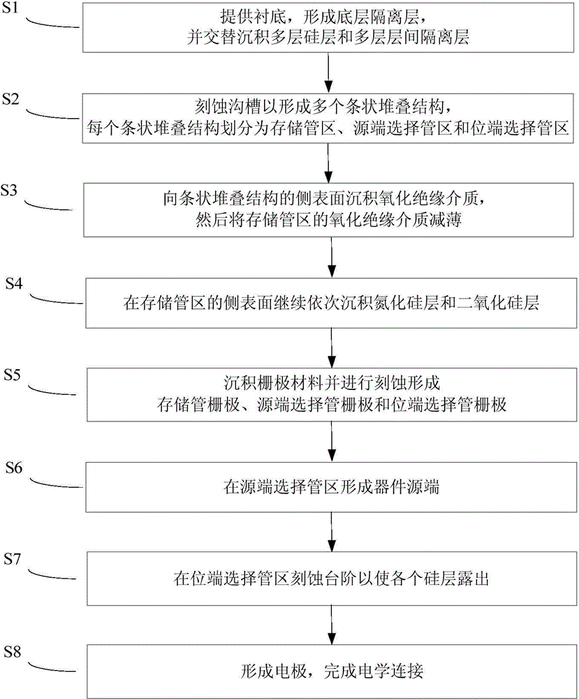
[0018] Such as figure 1 As shown, the method for forming a ladder-type vertical gate NAND according to the embodiment of the present invention may include the following steps S1 to S8:
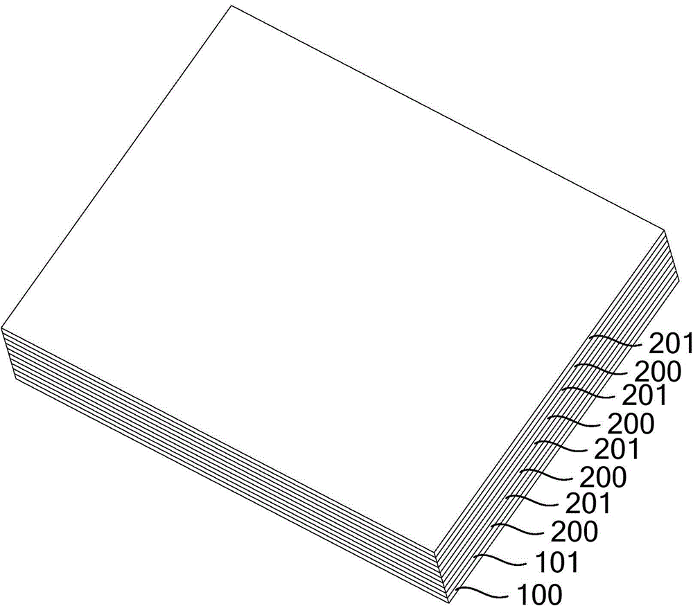
[0019] S1. Provide a substrate and form an underlying isolation layer on the substrate, and then alternately deposit multiple layers of silicon layers and multiple layers of interlayer isolation layers on the underlying isolation layer.
[0020] Specifically, such as Figure 2a to Figure 2d As shown, SiO can be formed on a substrate 100 of Si m...
PUM
 Abstract
Description
Claims
Application Information


