Insulated Gate Tunneling Groove Base Bipolar Transistor with Breakdown Protection

A bipolar transistor and breakdown protection technology, which is applied in semiconductor devices, semiconductor/solid-state device manufacturing, electrical components, etc., can solve the problem of increased static power consumption, increased sub-threshold swing of MOSFETs devices, and small forward conduction current, etc. question

Inactive Publication Date: 2018-05-22
SHENYANG POLYTECHNIC UNIV
View PDF3 Cites 0 Cited by
  • Summary
  • Abstract
  • Description
  • Claims
  • Application Information

AI Technical Summary

Problems solved by technology

In addition, the continuous shortening of the channel length has led to an increase in the subthreshold swing of MOSFETs, which has resulted in severe degradation of switching characteristics and a significant increase in static power consumption.
Although the degradation of device performance can be alleviated by improving the gate electrode structure, when the device size is further reduced to below 20 nanometers, even with the optimized gate electrode structure, the subthreshold swing of the device will also decrease. increases with further reductions in the device channel length, resulting in further deterioration of the device performance
[0003] Tunneling Field Effect Transistors (TFETs), compared with MOSFETs, although its average subthreshold swing has been improved, but its forward conduction current is too small. Narrow materials are used to generate the tunneling part of the tunneling field effect transistor, which can increase the tunneling probability to improve the transfer characteristics, but increases the difficulty of the process
In addition, the use of high dielectric constant insulating material as the insulating dielectric layer between the gate and the substrate can improve the control ability of the gate to the electric field distribution of the channel, but it cannot substantially increase the tunneling probability of the silicon material, so For the transfer characteristics of tunneling field effect transistors, the improvement is very limited
[0004] In addition, since tunneling field effect transistors and MOSFETs control the electric field, potential and carrier distribution inside the gate insulating layer and semiconductor through the electric field effect of the gate electrode, in order to improve the control ability of the gate electrode on the inside of the semiconductor, it is necessary to High dielectric constant and thinning gate insulating layer are used to enhance the control ability of the gate electrode, but at the same time, a large gate-induced drain leakage (GIDL) current will be generated when the gate is reverse-biased or Gate Induced Source Leakage (GISL) current

Method used


Image

  • Insulated Gate Tunneling Groove Base Bipolar Transistor with Breakdown Protection
  • Insulated Gate Tunneling Groove Base Bipolar Transistor with Breakdown Protection
  • Insulated Gate Tunneling Groove Base Bipolar Transistor with Breakdown Protection

Examples


Embodiment Construction

[0075] Below in conjunction with accompanying drawing, the present invention will be further described:

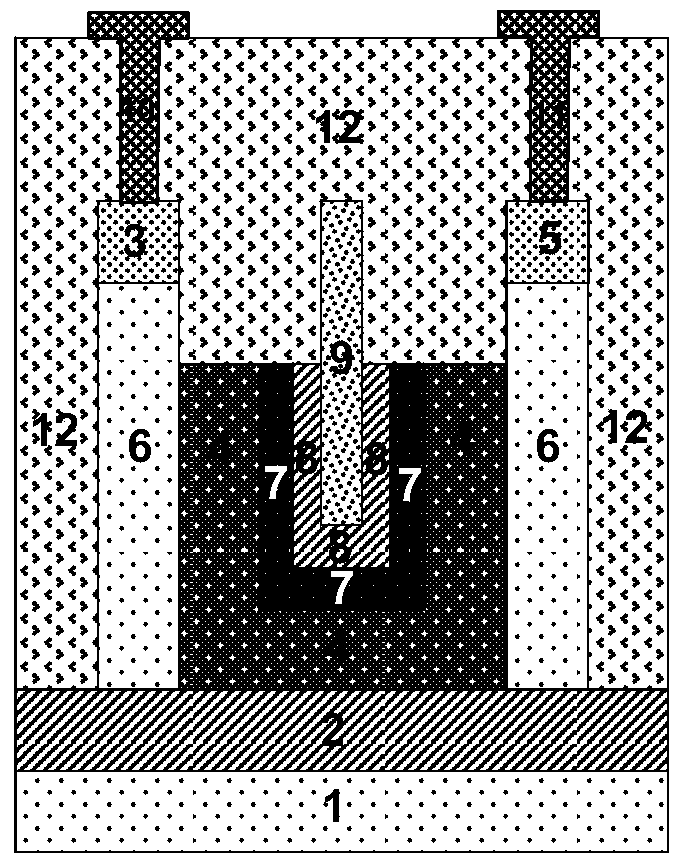
[0076] Such as figure 1 It is a schematic diagram of a two-dimensional structure of a gate-insulated tunneling groove base bipolar transistor with a breakdown protection function formed on an SOI substrate; specifically, it includes a single crystal silicon substrate 1; a wafer insulating layer 2; and an emitter region 3 ; Base region 4; Collector region 5; Breakdown protection region 6; Conductive layer 7; Tunneling insulating layer 8; Gate electrode 9; Emitter 10;

[0077] A gate-insulated tunneling groove base bipolar transistor with a breakdown protection function adopts a bulk silicon wafer containing only a single-crystal silicon substrate 1 as a device substrate, or adopts a single-crystal silicon The SOI wafer of the round insulating layer 2 is used as the substrate for generating the device; the base region 4 is located above the single crystal silicon substrate ...


PUM


Abstract

The invention relates to a gate insulation tunneling groove base bipolar transistor with a breakdown protection function. Compared with MOSFETs or tunneling field effect transistors of the same size, the breakdown by introducing a low impurity concentration into the collector junction and the emitter junction The protection zone can significantly improve the forward withstand voltage and reverse withstand voltage capabilities of the device at the deep nanoscale; use the extremely sensitive relationship between the impedance of the tunneling insulating layer and its internal field strength to achieve better switching characteristics; use the gate insulation tunneling The pass-through current is used as the driving current to induce the emitter-collector current, which realizes higher forward conduction characteristics; effectively suppresses the reverse leakage current caused by the tunneling effect between semiconductor bands and reduces the chip occupied by a single transistor by adopting a groove structure area. In addition, the invention also proposes a specific manufacturing method of the transistor, so it is suitable for popularization and application.

Description

Technical field: [0001] The invention relates to the field of ultra-large-scale integrated circuit manufacturing, and relates to a gate insulation tunneling groove base bipolar transistor with a breakdown protection function suitable for manufacturing high-performance ultra-high integrated integrated circuits. Background technique: [0002] At present, with the continuous improvement of the integration level, the source electrode and the channel or between the drain electrode and the channel of the integrated circuit unit Metal Oxide Semiconductor Field Effect Transistor (MOSFETs) devices form a steep mutation PN within a few nanometers. Junction, when the drain-source voltage is large, this steep abrupt PN junction will have a breakdown effect, which will cause the device to fail. As the size of the device continues to shrink, this breakdown effect becomes more and more obvious. In addition, the continuous shortening of the channel length leads to the increase of the sub-th...

Claims


Application Information

Patent Timeline
Patent Type & Authority Patents(China)
IPC IPC(8): H01L29/739H01L29/06H01L21/336
CPCH01L29/0684H01L29/66931H01L29/739
Inventor 靳晓诗刘溪
Owner SHENYANG POLYTECHNIC UNIV
Why Eureka
Try Eureka