Eureka AIR delivers breakthrough ideas for toughest innovation challenges, trusted by R&D personnel around the world.

Copper plating device and electroplating method for printed circuit board with through holes

A printed circuit board and copper plating technology, which is applied in plating tanks, electrolytic processes, electrolytic components, etc., can solve problems such as poor uniformity of micropores with high thickness-to-diameter ratio, different update rates of electrolytes, and influence of electroplating uniformity, etc., to achieve Improve the uniformity of electroplating and the quality of the plated parts, increase the deposition rate of the coating, and improve the effect of labor efficiency

Inactive Publication Date: 2017-02-22
UNIV OF ELECTRONIC SCI & TECH OF CHINA
View PDF7 Cites 2 Cited by
  • Summary
  • Abstract
  • Description
  • Claims
  • Application Information

AI Technical Summary

Problems solved by technology

But in the implementing device announced by this patent, its plated parts are vertically placed between the left chamber and the right chamber of the electroplating tank, and different holes are in different liquid levels on the printed circuit board plated parts with through holes in the same piece, which is subjected to The hydraulic pressure is different, so that the electrolyte update rate in different micropores is different, which affects the uniformity of the plating of the entire plate. In addition, the invention uses a mechanical method to seal the cathode plated parts, and the replacement of the plated parts is very complicated.
[0004] To sum up, at present, there are technical problems in through-hole plating of printed circuit boards, such as poor deep plating ability, poor uniformity of coating, poor uniformity of micropores with high thickness-to-diameter ratio, and difficulty in replacing plated parts.

Method used


Image

  • Copper plating device and electroplating method for printed circuit board with through holes
  • Copper plating device and electroplating method for printed circuit board with through holes
  • Copper plating device and electroplating method for printed circuit board with through holes

Examples


Embodiment Construction

[0027] Specific implementation examples

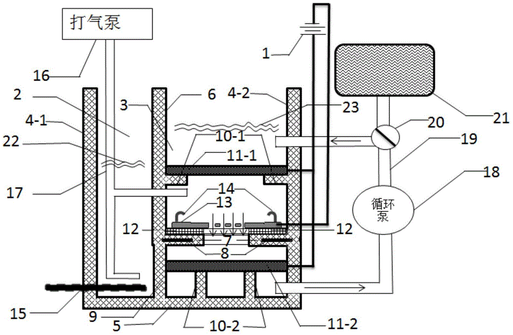
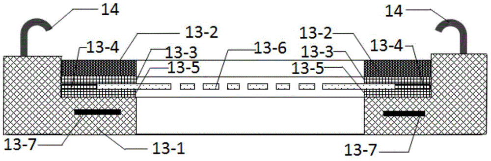
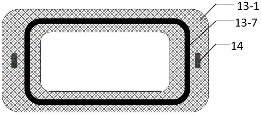
[0028] Such as figure 1 A copper plating device for through-holes of printed circuit boards with flowing electrolyte is shown, including: power supply (1), outer tank (2), inner tank (3), outer tank bottom (5), inner tank bottom (7), Magnetic body (8), inner tank support (9), upper anode support (10-1), lower anode support (10-2), upper anode (11-1), lower anode (11-2), elastic washer ( 12), cathode assembly (13), constant temperature heating device (15), air pump (16), air pipe (17), electrolyte circulation pump (18), electrolyte circulation pipe (19), tee (20) and reservoir (21). In consideration of material saving, the outer tank and the inner tank can share a part of the tank wall (4-2).

[0029] The bottom of the inner tank (7) is embedded with a magnetic body (8) and has a window, and the inner tank (3) is supported and fixed in the outer tank (2) by the inner tank bracket (9) placed on the bottom of the outer tank (5); The u...


PUM


Abstract

The invention belongs to the field of printed circuit board manufacturing, and relates to a metallization processing method and equipment for through holes of printed circuit boards, in particular to a copper plating device for through holes. A copper plating device for a printed circuit board with a through hole provided by the present invention includes a power supply, an outer tank, an inner tank, an inner tank bracket, an upper anode bracket, a lower anode bracket, an upper anode, a lower anode, an elastic washer, and a cathode assembly Components, constant temperature heating device, air pump, air pipe, electrolyte circulation pump, electrolyte circulation pipe, tee and liquid storage tank. The device can not only realize the through-hole plating of printed circuit boards with high thickness-to-diameter ratio, but also has excellent deep-plating ability, and at the same time greatly improves the uniformity of plating on the entire board, and has the advantages of convenient operation and high labor efficiency.

Description

technical field [0001] The invention belongs to the field of printed circuit board manufacturing, and relates to a metallization processing method and equipment for through holes of printed circuit boards, in particular to a copper plating device for through holes. Background technique [0002] With the advancement of electronic technology, one of the key components in electronic equipment - printed circuit boards have also developed from single-sided boards to double-sided boards and multi-layer boards. In multilayer printed circuit boards, interlayer circuits are connected through metal micro-holes. At present, in the field of printed circuit boards, the technologies for realizing micro-hole metallization mainly include electroless plating technology, electroplating technology, black hole electroplating technology and conductive material plugging technology, among which the former two are the mainstream technologies in the industry. It can be seen that the electroplating ...

Claims


Application Information

Patent Timeline
IPC IPC(8): C25D7/00C25D3/38C25D17/02C25D17/06C25D21/10C25D21/00
Inventor 王守绪陈国琴何为周国云王翀冀林仙陶志华
Owner UNIV OF ELECTRONIC SCI & TECH OF CHINA
Why Eureka
Eureka Blog
Learn More