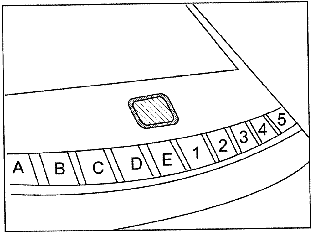
sensor
A technology of sensors and components, applied in the direction of instruments, computing, electrical digital data processing, etc., can solve the problems of high waste quantity and manufacturing cost
- Summary
- Abstract
- Description
- Claims
- Application Information
AI Technical Summary
Problems solved by technology
Method used
Image
Examples
Embodiment Construction
[0008] figure 1 The OFN shown in includes the middle region and the edges. The middle area is black, the edges should have a chrome look in daylight and backlit in low ambient light. Therefore, the edge must be at least partially transparent to visible light. The intermediate region must be transparent to infrared radiation in order to function as an OFN. Radiation having a wavelength of greater than 780 nm and preferably less than 1400 nm is considered to be infrared radiation in the sense of the present invention.
[0009] Black-dyed polycarbonate was used for the middle area and clear polycarbonate was used for the edges. These can be flushed together. After rinsing, the components are cleaned in ultrasonic electrolyte baths and subsequently dried. The central region is now covered, ie covered, for example by means of gluing, since the central region is not coated with a metal layer. Only the edges are exempt from masking.
[0010] The components are then coated with...
PUM
| Property | Measurement | Unit |
|---|---|---|
| Thickness | aaaaa | aaaaa |
Abstract
Description
Claims
Application Information
