Buried resistance printed board and manufacturing method thereof

A manufacturing method and technology of printed boards, which are applied in directions including printed resistors, printed circuit manufacturing, and printed electrical components, can solve problems such as occupying surface space, improve stability, avoid occupying surface space, and meet electrical requirements. The effect of sexual demands

Inactive Publication Date: 2015-03-18
SHENZHEN SUNTAK MULTILAYER PCB
View PDF7 Cites 13 Cited by
  • Summary
  • Abstract
  • Description
  • Claims
  • Application Information

AI Technical Summary

Problems solved by technology

[0003] The purpose of the present invention is to provide a buried resistance printed board and its manufacturing method, aiming to solve the problem that the external resistance components in the existing circuit board occupy a large amount of surface space

Method used


Image

  • Buried resistance printed board and manufacturing method thereof
  • Buried resistance printed board and manufacturing method thereof
  • Buried resistance printed board and manufacturing method thereof

Examples


Embodiment Construction

[0027] In order to make the object, technical solution and advantages of the present invention clearer, the present invention will be further described in detail below in conjunction with the accompanying drawings and embodiments. It should be understood that the specific embodiments described here are only used to explain the present invention, not to limit the present invention.

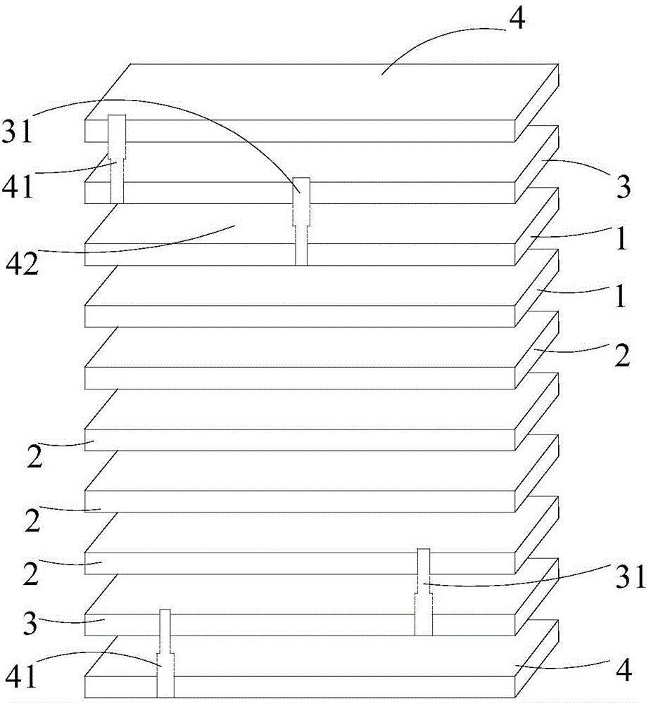
[0028] see figure 1 as well as figure 2 , an embodiment of the present invention provides a method for manufacturing a buried resistance printed board, comprising the following steps:

[0029] (1) Take a number of boards and cut each board so that each board meets the relevant specifications of the printed board. Divide the cut boards into four groups, which are the first board 1 and the second board. 2. The third plate 3 and the fourth plate 4, wherein the first plate 1 and the second plate 2 are multiple pieces, and the third plate 3 and the fourth plate 4 are two pieces, and the middle of eac...


PUM


Abstract

The invention relates to a printed board, provides a manufacturing method for a buried resistance printed board, and provides a buried resistance printed board manufactured by adopting the manufacturing method. According to the manufacturing method, a resistor is arranged on the inner layer of the printed board by etching, and good electrical conduction is formed through etched relevant circuits, blind holes and the like, so that the electrical requirement of the printed board is met, the surface space of the printed board is not occupied, and the miniaturization and multifunctional development of the printed board are facilitated; when each plate is laminated, the surfaces of inner layer plates are subjected to brown oxidation, so that bonding force among the plates can be improved; the printed board manufacturing by adopting the method is simple in structure, is large in surface space, and can be applied to various electronic products.

Description

technical field [0001] The invention relates to a printed board, in particular to a buried resistance printed board and a manufacturing method thereof. Background technique [0002] With the development of electronic products in the direction of miniaturization and multi-function, printed boards are also developing in the direction of miniaturization and high density. Most of the existing printed boards are separately installed between the resistance components and the printed board, and multiple resistance components are welded or inserted on the printed board, which greatly occupies the surface space of the circuit board, which is not conducive to the printed board. miniaturization development. Contents of the invention [0003] The object of the present invention is to provide a buried resistance printed board and its manufacturing method, aiming at solving the problem that the external resistance components in the existing circuit board occupy a large amount of surfac...

Claims


Application Information

Patent Timeline
IPC IPC(8): H05K1/16H05K3/46
CPCH05K1/167H05K3/4632
Inventor 杨巧云宋建远朱拓鲁惠
Owner SHENZHEN SUNTAK MULTILAYER PCB
Why Eureka
Try Eureka