A layout processing method for improving photolithography process window

A processing method and technology of photolithography technology, applied in the field of semiconductor manufacturing, can solve the problems of exposing active regions or polysilicon patterns, reducing the yield of finished products, and defects of finished products, so as to reduce the risk of defects, improve the yield of finished products, and increase the optical quality. The effect of engraving the process window

Active Publication Date: 2017-01-04
SHANGHAI HUALI MICROELECTRONICS CORP
View PDF12 Cites 0 Cited by
  • Summary
  • Abstract
  • Description
  • Claims
  • Application Information

AI Technical Summary

Problems solved by technology

[0003] In view of this, the present invention proposes a layout processing method for improving the photolithographic process window, so as to solve the problem that the size error of the photoresist pattern boundary is so large that the active area or polysilicon pattern is exposed, which will lead to subsequent product defects and reduce the quality of the finished product. rate problem

Method used


Image

  • A layout processing method for improving photolithography process window
  • A layout processing method for improving photolithography process window
  • A layout processing method for improving photolithography process window

Examples


Embodiment 1

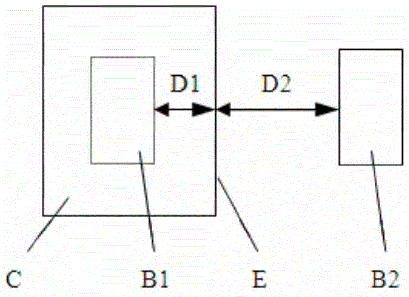
[0026] Please refer to FIG. 1a to FIG. 2b, a layout processing method for improving the photolithography process window of the present invention includes the following steps:

[0027] providing a photolithographic layout, and the photolithographic layout includes a photolithographic layout pattern of a shallow ion implantation layer;

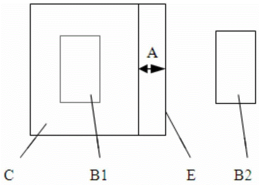
[0028] Find the graphic boundary E falling on the shallow trench isolation region from the photolithographic layout graphics; and the distance from the graphic boundary E to the first front-layer graphic B1 located in the photoresist open area C is the first dimension D1, and at the same time to the first front layer graphic B1 located in the photoresist open area C. The distance of the second front-layer pattern B2 in the photoresist-covered area is the second dimension D2;

[0029] Among them, if the value of the first dimension D1 is smaller than the value of the second dimension D2, the graphic boundary E is moved towards the direction of th...

Embodiment 2

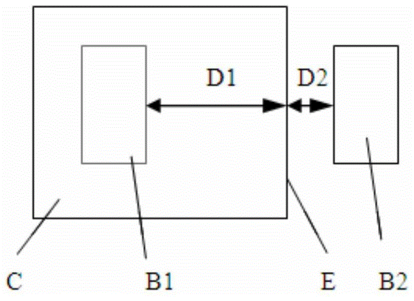
[0048] See Figures 2a and 2b:

[0049] The photolithography layout pattern of the ion implantation layer, the open area of ​​the photoresist pattern is C, and the other area is the coverage area of ​​the photoresist pattern;

[0050] Step 1: Select the pattern boundary E that falls on the shallow trench isolation region, and its distance to the front-layer pattern B1 in the open area C of the photoresist pattern satisfies D1, and the distance to the front-layer pattern in the photoresist pattern coverage area The distance of B2 satisfies D2;

[0051] D1 needs to be selected and adjusted according to the design rules and actual process capabilities, and is the distance from the graphic boundary E to the front-layer graphic B1 in the photoresist pattern opening area C, which is used to select whether it does not meet or is not conducive to the actual process requirements, or is sufficient The boundary that satisfies or far satisfies the actual process requirements; D2 needs to be...


PUM


Abstract

The invention discloses a layout treatment method for adding a photoetching process window. The layout treatment method comprises the following steps: providing a photoetching layout pattern with a shallow ion-implanted layer; finding a pattern boundary falling in a shallow groove insulation area from the photoetching layout pattern, wherein the distance from the pattern boundary to a first front layer pattern positioned in a photoresist open area is a first dimension, and the distance from the pattern boundary to a second front layer pattern positioned in a photoresist coverage area is a second dimension; and if the value of the first dimension is less than the value of the second dimension, moving the pattern boundary towards the direction of the second front layer pattern by a distance A1, if not, moving the pattern boundary towards the direction of the first front layer pattern by a distance A2, wherein the value of the A1 is less than the value of the second dimension, and the value of the A2 is less than the value of the first dimension. The layout treatment method disclosed by the invention can achieve the effect of adding the photoetching process window by utilizing the surplus distance space of a shallow ion-implanted layer layout, and can not influence parts because the ion implantation in the shallow groove insulation area is ineffective, and thus the risk of causing defects due to pattern distortion is effectively reduced and the finished product qualification rate is increased.

Description

technical field [0001] The invention relates to the technical field of semiconductor manufacturing, in particular to a layout processing method for improving a photolithography process window. Background technique [0002] Since the front layer of the semiconductor is a variety of substrates and undulating topography, the photolithography pattern of the ion implantation layer is affected by the substrate and its topography, and the pattern size will be distorted, resulting in line width deformation and a reduction in the photolithography process window. Small, resulting in defects, thereby reducing the yield of finished products. In the rule-based optical proximity correction method, the number of test patterns needs to be doubled to increase the pattern coverage when a variety of substrates and undulating shapes are used, which greatly increases time and labor costs; while the model-based optical proximity correction method cannot accurately predict complex The case of the...

Claims


Application Information

Patent Timeline
Patent Type & Authority Patents(China)
IPC IPC(8): G03F9/00
Inventor 张月雨于世瑞
Owner SHANGHAI HUALI MICROELECTRONICS CORP
Why Eureka
Try Eureka