Pressing and fixing assembly used for packaging transistors

A technology for fixing components and transistors, which is used in semiconductor/solid-state device manufacturing, semiconductor/solid-state device components, and electrical solid-state devices. Production management costs, great process complexity, and the effect of reducing the size of the whole machine

Active Publication Date: 2015-03-25
GOODWE TECHNOLOGIES CO LTD
View PDF5 Cites 4 Cited by
  • Summary
  • Abstract
  • Description
  • Claims
  • Application Information

AI Technical Summary

Problems solved by technology

[0005] 3. PCBA does not open holes, transistors are reversed, and manual secondary soldering, such as image 3 As shown, for this structure, the secondary manual soldering of transistor 5 is slightly worse in consistency and cost than machine soldering. There is no need to add intermediate transition heat sinks, and the heat dissipation performance of transistor 5 is improved. PCBA board 2 is only installed with screws. hole, the size of the PCBA board 2 is reduced, the cost is significantly reduced, the size of the whole machine can be reduced by more than 19.5% (69 / 335), the strength of the PCBA board 2 will not be reduced, because there is no hole for installation, and the soldering of the transistor 5 needs to be pre-processed section, and special fixtures are required. During the pre-processing process, the metal shrapnel 7 needs to be fixed on the fixture to ensure the height and position of the transistor 5 after welding. After the welding is completed, it is disassembled and then reassembled and fixed in the whole machine. Because it is a reverse assembly, it is necessary to ensure that the relative positions of the shrapnel, the transistor and the PCBA cannot be shifted. Otherwise, it is difficult to align the metal shrapnel hole and the radiator screw hole during assembly. However, with this structural design, the metal shrapnel 7 and the transistor 5 cannot be aligned. The structure of the limit position, the pre-fixation of the two is very difficult to achieve, even if a special fixture is used, it is difficult to process, and it involves the electrical safety of other plug-in pins of the PCBA board 2 and the metal shrapnel 7, it is necessary to increase the insulating sheet 14, resulting in the entire assembly process. It is very complicated, the process takes a long time, and it is difficult to maintain and replace later. This type of structure is rarely used at present
[0006] 4. PCBA does not open holes, transistors are reversed, and manual secondary soldering, such as Figure 4 As shown, for this structure, the secondary manual soldering of transistor 5 is slightly worse in consistency and cost than machine soldering. There is no need to add intermediate transition heat sinks, and the heat dissipation performance of transistor 5 is improved. PCBA board 2 is only installed with screws. hole, the size of PCBA board 2 is reduced, and the cost is significantly reduced. The size of the whole machine can be reduced by more than 20%, and the strength of PCBA will not be reduced. Because there is no hole for installation, the welding of transistor 5 needs to be placed in the pre-processing section, which requires fixtures and pre-processing During the process, the plastic pressing part 6 needs to be fixed on the jig to ensure the height and position of the transistor 5 after welding. After the welding is completed, it is disassembled and then reassembled and fixed in the whole machine. This structural plastic pressing part 6 and transistor 5 needs to be fixed carefully, and the height tolerance is large (0-0.6); the use of plastic parts does not need to consider the electrical safety of the PCBA board 2 plug-in pins, but the use of plastic parts as compression parts has poor elasticity and small deformation. The reliability is poor under the shock of vibration and the heat and cold of the transistor; in addition, the lifespan of plastic is much worse than that of metal shrapnel in a long-term high-temperature and high-humidity environment; Parts are cracked, and it is difficult to check, and the assembly process is more complicated. This kind of structure has been widely used in domestic photovoltaic inverters before, and the metal shrapnel structure is gradually being adopted at present.
[0007] In summary, the current photovoltaic inverter or other power supply industries basically adopt the above-mentioned structural scheme, or a single optimized and improved structure derived from the above-mentioned structure, but in terms of comprehensive performance such as cost, size, process, reliability, and life Look, none of the above solutions or a single optimization solution can solve these problems very well

Method used


Image

  • Pressing and fixing assembly used for packaging transistors
  • Pressing and fixing assembly used for packaging transistors
  • Pressing and fixing assembly used for packaging transistors

Examples


Embodiment Construction

[0039] The present invention will be described in detail below with reference to the accompanying drawings and in combination with embodiments.

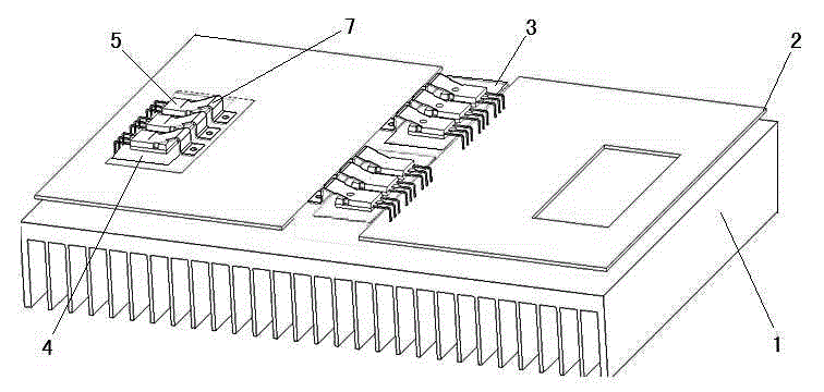
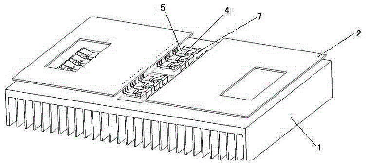
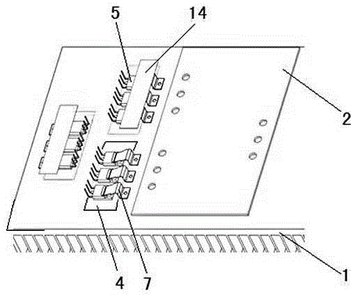
[0040] refer to figure 1As shown, a pressing and fixing assembly for packaging transistors includes a PCBA board 2 and a transistor 5. The pressing and fixing assembly includes a combined metal spring 7 and a plastic fixing part 8, and the plastic fixing part 8 is composed of a side wall Form a cavity with the bottom wall, the inner wall of the cavity and / or the inner bottom wall are provided with an inner buckle 9 and a support rib 10, and the metal shrapnel 7 is fixed on the plastic fixing part by being inserted between the inner buckle 9 and the support rib 10 8, a supporting step 11 is provided on the inner wall and / or inner bottom wall of the cavity, and an outer buckle 12 extending outward along the opposite direction of the metal dome 7 is provided on the outer bottom wall of the cavity.

[0041] It also includes the assembly...


PUM


Abstract

The invention relates to a pressing and fixing assembly used for packaging transistors. The pressing and fixing assembly comprises a PCBA board, the transistors, metal elastic pieces and plastic fixing parts, wherein the metal elastic pieces and the plastic fixing parts are combined together. A containing cavity is formed by the side wall and the bottom wall in each plastic fixing part, inner buckles and supporting ribs are arranged on the inner side wall and / or the inner bottom wall of each containing cavity, the metal elastic pieces are inserted between the inner buckles and the supporting ribs to be fixed on the plastic fixing parts, a supporting step is arranged on the inner side wall and / or the inner bottom wall of each containing cavity, and outer buckles are arranged on the outer bottom wall of each containing cavity and extend outwards in the reverse direction of the corresponding metal elastic piece. By the adoption of the technical scheme, the size of the PCBA board is greatly reduced, the size of a complete machine is reduced, the material cost of the complete machine is reduced obviously, the heat dissipation stability and the reliability are high, the pressing and fixing assembly is low in cost, the technological complexity of the welding process can be greatly lowered, the technological time is shortened, the defect rate in the process is decreased, and the production management cost is reduced.

Description

technical field [0001] The invention belongs to the technical field of switching power supplies and photovoltaic inverters, and is applied to the T0247 packaging used in current AC-DC conversion or similarly packaged transistors for heat dissipation, pressing and fixing, and specifically relates to a pressing and fixing assembly for packaging transistors. Background technique [0002] At present, in the field of photovoltaic inverters, there are mainly the following methods for the assembly, heat dissipation, compression and fixing of transistors and PCBA boards: [0003] 1. PCBA opening, transistor mounting, wave soldering, such as figure 1 As shown, for this structure, the machine welding of the transistor 5 has certain advantages in consistency, quality and cost, but it is necessary to increase the intermediate transition heat sink 3, so that the heat conduction resistance increases, and the heat dissipation performance of the transistor 5 decreases. In addition, the PCBA...

Claims


Application Information

Patent Timeline
Patent Type & Authority Applications(China)
IPC IPC(8): H01L21/58H01L23/13H01L23/40H05K13/04
CPCH01L21/67121H05K13/04
Inventor 戴飞雄刘建峰王涛
Owner GOODWE TECHNOLOGIES CO LTD
Why Eureka
Try Eureka