Semiconductor packaging piece and manufacturing method thereof

A manufacturing method and semiconductor technology, which are applied in the fields of semiconductor/solid-state device manufacturing, semiconductor devices, and semiconductor/solid-state device components, etc., can solve the problems of increased thickness of semiconductor packages, complicated processes, and increased costs.

Inactive Publication Date: 2015-03-25
SAMSUNG SEMICON CHINA RES & DEV +1
View PDF3 Cites 2 Cited by
  • Summary
  • Abstract
  • Description
  • Claims
  • Application Information

AI Technical Summary

Problems solved by technology

As the functions of chips become more and more powerful, the heat dissipation requirements for semiconductor packages are getting higher and higher, but the heat dissipation capability of traditional epoxy molding compounds is limited
[0003] Traditional epoxy molding compounds may have a planar (e.g., flat and smooth) structu

Method used


Image

  • Semiconductor packaging piece and manufacturing method thereof
  • Semiconductor packaging piece and manufacturing method thereof
  • Semiconductor packaging piece and manufacturing method thereof

Examples


Embodiment Construction

[0028] Hereinafter, the invention will be described more fully with reference to the accompanying drawings, in which embodiments of the invention are shown. This invention can be implemented in many different ways and should not be construed as limited to the embodiments set forth herein. In the drawings, the dimensions of layers and regions may be exaggerated for clarity.

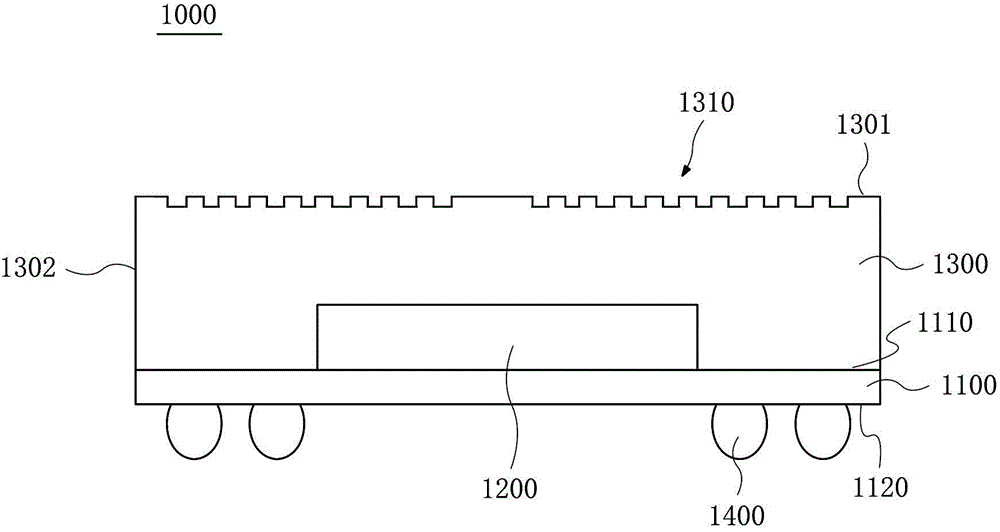
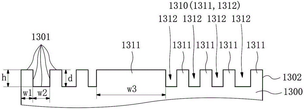
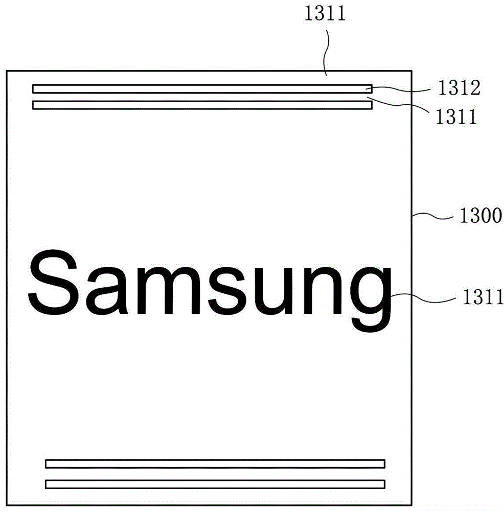
[0029] figure 1 is a schematic cross-sectional view showing a semiconductor package according to an exemplary embodiment of the present invention. figure 2 is a partially enlarged cross-sectional view illustrating an encapsulation member included in a semiconductor package according to an exemplary embodiment of the present invention. image 3 is a schematic plan view showing an encapsulation member included in a semiconductor package according to an exemplary embodiment of the present invention. refer to figure 1 , figure 2 and image 3 , a semiconductor package 1000 according to an exemplary embo...


PUM

PropertyMeasurementUnit
Heightaaaaaaaaaa

Abstract

The invention provides a semiconductor packaging piece and a manufacturing method thereof. The semiconductor packaging piece comprises a substrate, a semiconductor chip and a packaging component, wherein the substrate is provided with a first surface and a second surface opposite to the first surface; the semiconductor chip is mounted on the first surface of the substrate; the packaging component comprises a packaging semiconductor chip and an outer surface with a fine structure, and the fine structure has a nanometer size and comprises a boss and a dent which is arranged adjacent to the boss.

Description

technical field [0001] The present invention relates to a semiconductor package and a manufacturing method thereof, and more particularly to a semiconductor package in which an encapsulating member has a fine structure provided on an outer surface thereof and a manufacturing method thereof. Background technique [0002] A semiconductor package generally includes a chip and an encapsulation member such as epoxy molding compound (EMC) that encapsulates and protects the chip. Traditional epoxy molding compounds consist of cured epoxy resins and fillers such as silicon oxide. As the functions of chips become more and more powerful, the heat dissipation requirements for semiconductor packages are getting higher and higher. However, the heat dissipation capability of traditional epoxy molding compounds is limited. [0003] Conventional epoxy molding compounds may have a planar (eg, flat and smooth) structure with limited ability to dissipate heat. In addition, a large semiconduc...

Claims


Application Information

Patent Timeline
IPC IPC(8): H01L23/31H01L21/56H01L21/48
CPCH01L23/544H01L2223/54406H01L2223/5442H01L2223/54433H01L2223/54486H01L2924/15311H01L2924/1815
Inventor 王玉传
Owner SAMSUNG SEMICON CHINA RES & DEV
Why Eureka
Try Eureka