Thin film transistor array substrate, liquid crystal panel and liquid crystal display

A technology of thin film transistors and array substrates, applied in the field of liquid crystal display, can solve the problems of reducing the aperture ratio of the display and the performance of the display, and achieve the effect of improving the display quality and high aperture ratio

Active Publication Date: 2015-03-25
TCL CHINA STAR OPTOELECTRONICS TECH CO LTD
View PDF3 Cites 26 Cited by
  • Summary
  • Abstract
  • Description
  • Claims
  • Application Information

AI Technical Summary

Problems solved by technology

Due to the distance between the array substrate 1 and the filter substrate 2, the black matrix 22 needs to cover a larger area to prevent light leakage, which reduces the aperture ratio of the display.
[0005] In addition, if figure 1 In th

Method used


Image

  • Thin film transistor array substrate, liquid crystal panel and liquid crystal display
  • Thin film transistor array substrate, liquid crystal panel and liquid crystal display
  • Thin film transistor array substrate, liquid crystal panel and liquid crystal display

Examples


Embodiment Construction

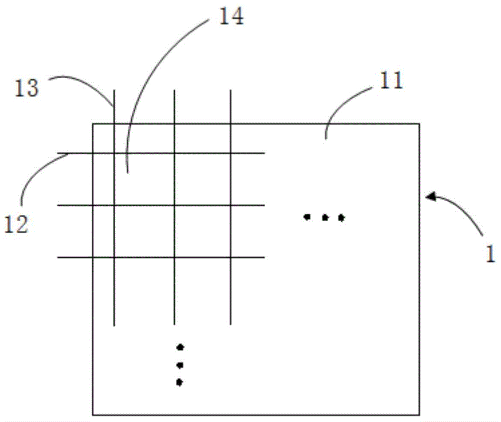
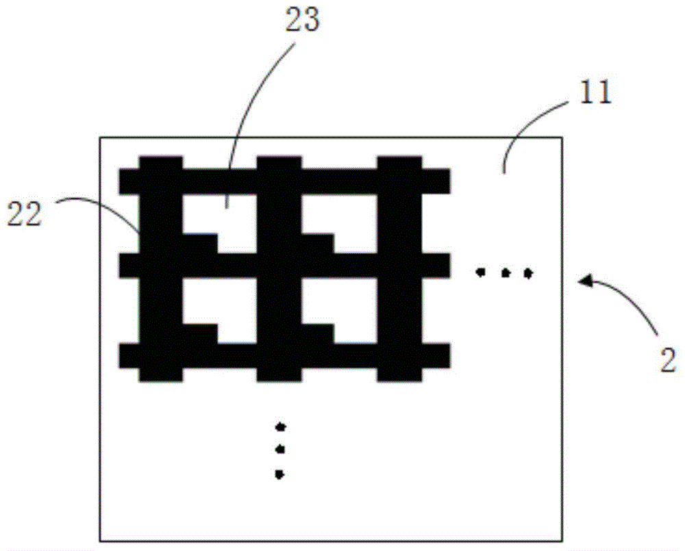
[0028] As mentioned above, the purpose of the present invention is to improve the traditional liquid crystal panel. When the black matrix used for light shielding is arranged on the filter substrate, due to the distance between the liquid crystal cells, the black matrix needs to cover a larger area to prevent light leakage. , the problem of reducing the aperture ratio of the display provides a thin film transistor array substrate and a liquid crystal panel including the array substrate, by setting a metal metal light-shielding layer above the thin film transistor array to replace the traditional black color on the filter substrate matrix, so that the pixel area of ​​the liquid crystal panel can obtain a higher aperture ratio. In addition, the metal light-shielding layer can block light from irradiating the active layer of the thin film transistor, thereby improving the display quality of the display device.

[0029] The technical solutions in the embodiments of the present inv...


PUM


Abstract

The invention discloses a thin film transistor array substrate. The thin film transistor array substrate comprises a first substrate, scanning lines, data lines and a pixel region, wherein the scanning lines and the data lines are located on the first substrate, and intersect to limit the pixel region. The pixel region comprises a thin film transistor and a pixel electrode located above the thin film transistor. A metal light-shielding layer is arranged between the thin film transistor and the pixel electrode, and comprises a first light-shielding region, a second light-shielding region and a third light-shielding region in a mutual isolation mode. The first light-shielding region is located between a source electrode/drain electrode and the pixel electrode, and the pixel electrode is electrically connected to the source electrode/drain electrode through the first light-shielding region. The second light-shielding region is located above an active layer, and the third light-shielding region is located above the scanning lines and the data lines. The invention further discloses a liquid crystal panel. The liquid crystal panel comprises the thin film transistor array substrate. The invention further discloses a liquid crystal display comprising the liquid crystal panel.

Description

technical field [0001] The invention relates to the technical field of liquid crystal display, in particular to a thin film transistor array substrate, a liquid crystal panel and a liquid crystal display. Background technique [0002] Liquid Crystal Display (LCD) is a flat and ultra-thin display device, and the liquid crystal panel is an important part of the liquid crystal display. [0003] refer to Figure 1-3 A common liquid crystal panel at least includes an array substrate 1 and a color filter substrate 2 oppositely arranged and a liquid crystal layer 3 between the array substrate 1 and the color filter substrate 2 . Wherein, the array substrate 1 includes a first substrate 11 , scan lines 12 and data lines 13 located on the first substrate 11 , and a pixel region 14 defined by intersections of the scan lines 12 and data lines 13 . Wherein, the pixel region 14 includes a thin film transistor 14a and a pixel electrode 14b located above the thin film transistor 14a. The...

Claims


Application Information

Patent Timeline
IPC IPC(8): H01L27/12H01L23/552G02F1/1362G02F1/1368
CPCH01L23/552H01L2924/0002H01L29/78633G02F1/136209G02F1/136227H01L27/124H01L27/1248H01L2924/00G02F1/133514G02F1/134309G02F1/1345G02F1/136286G02F1/1368G02F2201/121G02F2201/123
Inventor 黄秋平
Owner TCL CHINA STAR OPTOELECTRONICS TECH CO LTD
Why Eureka
Try Eureka