Back-contact heterojunction solar cell and manufacturing method thereof

A solar cell and heterojunction technology, which is applied in the field of solar cells, can solve the problems of p-n junction quality degradation and reduced incident light absorption efficiency, etc.

Active Publication Date: 2015-03-25
TRINA SOLAR CO LTD
View PDF4 Cites 2 Cited by
  • Summary
  • Abstract
  • Description
  • Claims
  • Application Information

AI Technical Summary

Problems solved by technology

[0002] At present, the effective management of incident light is one of the technical difficulties of thin-film / crystalline silicon heterojunction solar cells. The absorption efficiency of incident light, however, due to the coplanar design of the emitter and the back field of the full back electrode structure, the quality of the p-n junction is reduced

Method used


Image

  • Back-contact heterojunction solar cell and manufacturing method thereof
  • Back-contact heterojunction solar cell and manufacturing method thereof

Examples


Embodiment Construction

[0025] In order to make the content of the present invention more clearly understood, the present invention will be further described in detail below based on specific embodiments and in conjunction with the accompanying drawings.

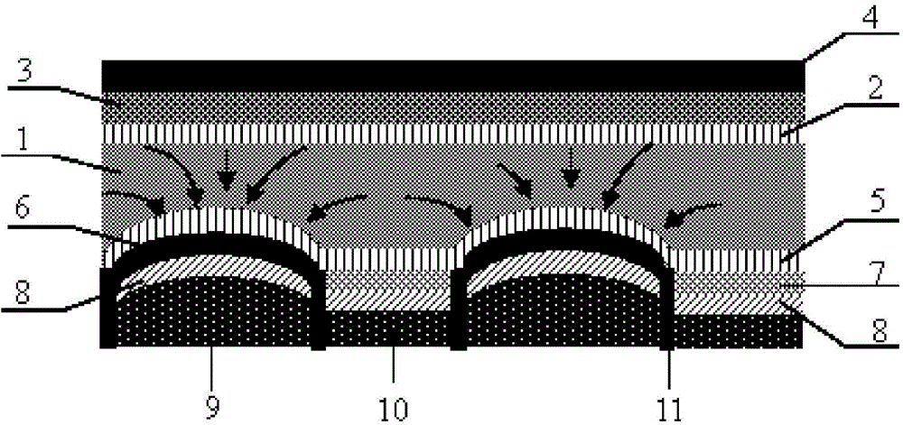
[0026] Such as figure 1 As shown, a back-contact heterojunction solar cell includes a silicon wafer base layer 1. The back side of the silicon wafer base layer 1 has a P-type contact area and an N-type contact area, and the P-type contact area is recessed toward the silicon wafer base layer 1. The inner curved surface structure, and the P-type contact area is the back intrinsic layer 5, the emitter 6, the conductive medium layer 8 and the emitter electrode 9 from the inside to the outside; the N-type contact area is the back intrinsic layer from the inside to the outside 5. Back electric field layer 7 , conductive medium layer 8 and back electric field electrode 10 .

[0027] Such as figure 1 As shown, the front surface of the substrate layer 1 o...


PUM


Abstract

The invention discloses a back-contact heterojunction solar cell and a manufacturing method thereof. The back-contact heterojunction solar cell comprises a silicon wafer base body layer, wherein a P type contact area and an N type contact area are arranged on the back side of the silicon wafer base body layer, the P type contact area is of a negative camber structure concave towards the silicon wafer base body layer, a back side intrinsic layer, an emitter, a conductive dielectric layer and an emitter electrode are arranged on the P type contact area from inside to outside in sequence, and a back side intrinsic layer, a back electric field layer, a conductive dielectric layer and a back electric field electrode are arranged on the N type contact area from inside to outside in sequence. According to the back-contact heterojunction solar cell and the manufacturing method thereof, the junction characteristic of the solar cell can be improved, wide-angle scattering of incident light inside a substrate is facilitated, the effective optical distance of an absorption layer is increased, and the overall performance of the solar cell is improved.

Description

technical field [0001] The invention relates to a back contact heterojunction solar cell and a preparation method thereof, belonging to the technical field of solar cells. Background technique [0002] At present, the effective management of incident light is one of the technical difficulties of thin-film / crystalline silicon heterojunction solar cells. However, due to the coplanar design of the emitter and the back field of the full back electrode structure, the quality of the p-n junction is reduced. Contents of the invention [0003] The technical problem to be solved by the present invention is to overcome the defects of the prior art and provide a back contact heterojunction solar cell, which can not only improve the junction characteristics of the back contact heterojunction solar cell, but also help the incident light The wide-angle scattering increases the effective optical path of the absorbing layer, thereby improving the overall performance of the battery. [0...

Claims


Application Information

Patent Timeline
Patent Type & Authority Applications(China)
IPC IPC(8): H01L31/0224H01L31/052H01L31/18
CPCH01L31/022441H01L31/18H01L31/186Y02E10/50Y02P70/50
Inventor 郭万武
Owner TRINA SOLAR CO LTD
Why Eureka
Try Eureka