Semiconductor photo-detecting device

一种光检测装置、半导体的技术,应用在半导体器件、光伏发电、可持续制造/加工等方向,能够解决检测准确性劣化等问题,达到低响应率的效果

Active Publication Date: 2015-03-25
SEOUL VIOSYS CO LTD
View PDF4 Cites 7 Cited by
  • Summary
  • Abstract
  • Description
  • Claims
  • Application Information

AI Technical Summary

Problems solved by technology

That is, commonly used semiconductor photodetection devices flow low currents in response to visible light rather than UV light, deteriorating detection accuracy

Method used


Image

  • Semiconductor photo-detecting device
  • Semiconductor photo-detecting device
  • Semiconductor photo-detecting device

Examples


Embodiment Construction

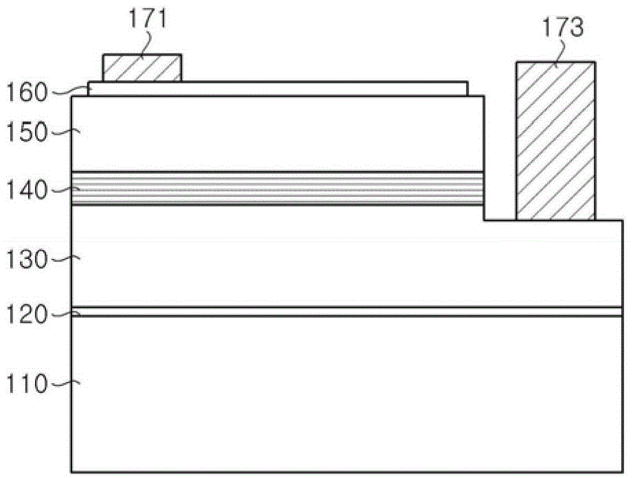
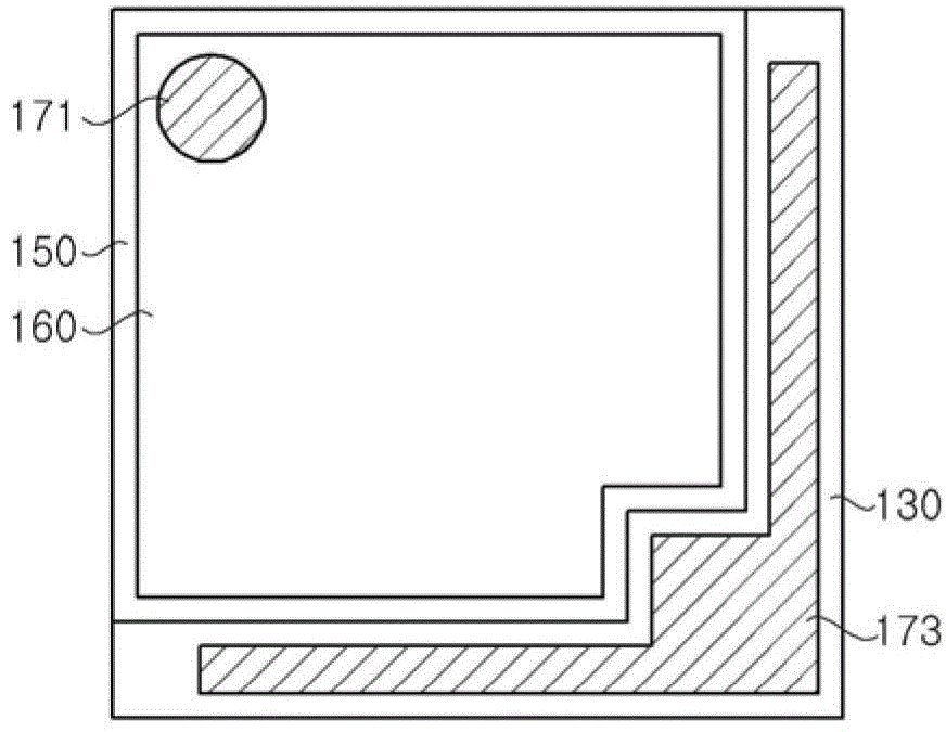
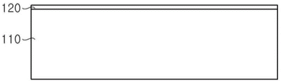
[0040] Hereinafter, embodiments of the present invention will be described in detail with reference to the accompanying drawings. The following embodiments are provided as examples in order to fully convey the spirit of the present invention to those skilled in the art to which the present invention pertains. Therefore, the present invention is not limited to the embodiments disclosed herein, and can also be implemented in various forms. In the drawings, the width, length, thickness, etc. of elements may be exaggerated for convenience. Also, when an element is referred to as being "on" or "on" another element, it can be "directly on" or "on" the other element or intervening elements may be present. It will be understood that for the purposes of this disclosure, "at least one of X, Y, and Z" may be construed to mean only X, only Y, only Z, or two or both of X, Y, and Z. Any combination of more terms (for example, XYZ, XYY, YZ, ZZ). Throughout the specification, the same refe...


PUM


Abstract

A photo-detecting device includes a first nitride layer, a low-current blocking layer disposed on the first nitride layer, a light absorption layer disposed on the low-current blocking layer, and a Schottky junction layer disposed on the light-absorption layer. The low-current blocking layer includes a multilayer structure.

Description

technical field [0001] The invention relates to a semiconductor light detection device. More particularly, the present invention relates to a semiconductor photodetection device having excellent detection efficiency for light of a specific wavelength. Background technique [0002] Semiconductor photodetection devices operate based on the principle that current is induced by illuminating light. In particular, semiconductor photodetection devices for detecting UV light are becoming important due to their application in various fields such as commerce, medicine, arms industry, communication, and the like. A semiconductor photodetection device is based on the principle that a depletion region is formed by separation of electrons and holes within a semiconductor according to the absorption of photons, thereby inducing a current according to the flow of electrons. [0003] In this field, semiconductor photodetection devices using silicon are generally used. However, such a semi...

Claims


Application Information

Patent Timeline
Patent Type & Authority Applications(China)
IPC IPC(8): H01L31/101
CPCH01L31/101H01L31/18H01L31/108H01L31/03044H01L31/03048H01L31/1856H01L31/1848Y02P70/50H01L31/09Y02E10/544
Inventor 朴起延金华睦李圭浩李晟贤金亨奎
Owner SEOUL VIOSYS CO LTD
Why Eureka
Try Eureka