AMOLED device structure and manufacturing method thereof

A technology of device structure and driving voltage, applied in the field of OLED display devices, can solve the problems of large resistance, poor uniformity and large difference in brightness of AMOLED screen, etc.

Active Publication Date: 2015-03-25
KUNSHAN GO VISIONOX OPTO ELECTRONICS CO LTD
View PDF5 Cites 13 Cited by
  • Summary
  • Abstract
  • Description
  • Claims
  • Application Information

AI Technical Summary

Problems solved by technology

In a top-emitting AMOLED, the cathode layer is usually a thin film formed of metals such as Mg and Ag. Because it needs to have light-transmitting properties, it must be made very thin, resulting in high resistance.
The cathode layer is connected to the negative driving voltage wiring around the substrate. If the cathode resistance is large, the difference between the cathode voltage near the substrate and the cathode voltage in the middle of the substrate will be large, resulting in poor brightness uniformity of the AMOLED screen.
Especially for large-size AMOLED devices, this problem is more obvious

Method used


Image

  • AMOLED device structure and manufacturing method thereof
  • AMOLED device structure and manufacturing method thereof
  • AMOLED device structure and manufacturing method thereof

Examples


Embodiment Construction

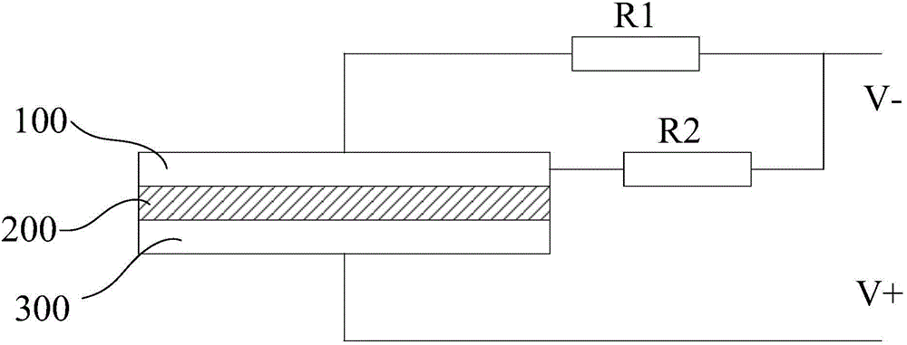
[0026] Such as figure 1 Shown is a schematic diagram of reducing the resistance of the cathode layer of the AMOLED display. The AMOLED display screen includes an AMOLED device structure and other related components. The AMOLED device structure includes a cathode layer 100 , an organic light emitting layer 200 and an anode layer 300 stacked in sequence. The cathode layer 100 is connected to the negative electrode of the driving voltage V−, and the anode layer 300 is connected to the positive electrode of the driving voltage V+. The driving voltage excites the organic light emitting layer 200 to emit light to form a pixel to emit light. The sub-pixels of each pixel unit use the same cathode voltage and different anode voltages to make the sub-pixels emit color light with different brightness. Since different points on the cathode layer 100 have different distances from the connection terminal of the negative electrode of the driving voltage at the edge of the display screen, ...


PUM


Abstract

The invention discloses an AMOLED device structure. The AMOLED device structure comprises a driving voltage device, a cathode layer, an organic light-emitting layer and an anode layer, wherein the cathode layer, the organic light-emitting layer and the anode layer are sequentially arranged in an overlapped mode, the cathode layer is connected with the negative pole of the driving voltage device, and the anode layer is connected with the positive pole of the driving voltage device. The AMOLED device structure is characterized by further comprising a cathode auxiliary layer, and the cathode auxiliary layer is connected with the cathode layer and the negative pole of the driving voltage device. The invention further discloses a manufacturing method of the AMOLED device structure. According to the AMOLED device structure and the manufacturing method of the AMOLED device structure, as the cathode auxiliary layer is arranged in an original structure, the problem that cathode resistance is too large because a cathode is thin or a display screen is large in size can be solved.

Description

technical field [0001] The invention relates to an OLED display device, in particular to an AMOLED device structure and a manufacturing method thereof. Background technique [0002] AMOLED (Active Matrix Organic Light Emitting Diode, Active Matrix Organic Light Emitting Diode), compared with traditional LCD panels, has many advantages such as low drive, low power consumption, self-illumination, fast response, high contrast, and wide viewing angle. won widespread attention. [0003] In traditional technology, AMOLED usually consists of an anode layer, a cathode layer, and an organic light-emitting layer sandwiched between the anode layer and the cathode layer. When appropriate voltages are applied to the anode layer and the cathode layer, the middle organic light-emitting layer is excited to emit light autonomously. In a top-emitting AMOLED, the cathode layer is usually a thin film formed of metals such as Mg and Ag, which is made very thin due to its light-transmitting pro...

Claims


Application Information

Patent Timeline
Patent Type & Authority Applications(China)
IPC IPC(8): H01L51/52H01L51/56
CPCH10K50/80H10K50/824H10K2102/302H10K71/00
Inventor 赵海廷魏朝刚刘青刚
Owner KUNSHAN GO VISIONOX OPTO ELECTRONICS CO LTD
Why Eureka
Try Eureka