Welding structure at tail of touch control film

A welding structure and touch film technology, applied in the electronic field, can solve the problems of increased packaging materials and transportation costs, increased production costs, and difficulty in ensuring accuracy, and achieve the goals of reducing costs and transportation costs, saving production costs, and ensuring welding accuracy Effect

Inactive Publication Date: 2015-04-08
罗延廷
View PDF5 Cites 0 Cited by
  • Summary
  • Abstract
  • Description
  • Claims
  • Application Information

AI Technical Summary

Problems solved by technology

[0007] However, in the existing technology, soldering of the touch film is prone to false welding, and the base of the pad cannot be bent, which affects the overall bending performance of the touch film. In addition, the pad is long and strip-shaped and cannot be bent, resulting in a flicking of the long side of the package. When the film is used, the volume of the packaging barrel required is huge, and the packaging material and transportation costs must be doubled, which increases the production cost; in addition, the soldering is mainly manual operation, and the accuracy is difficult to guarantee, resulting in a high defective rate and high temperature. It is easy to cause deformation of the film during soldering, and if an additional process is added in the production process of the touch film --- paste the insulating strip, and because the place where the insulating strip is pasted cannot naturally bend with the touch film, it may cause the user Many inconveniences when using the touch film

Method used


Image

  • Welding structure at tail of touch control film
  • Welding structure at tail of touch control film

Examples


Embodiment Construction

[0017] The present invention will be further described in detail below in conjunction with the accompanying drawings, so that those skilled in the art can implement it with reference to the description.

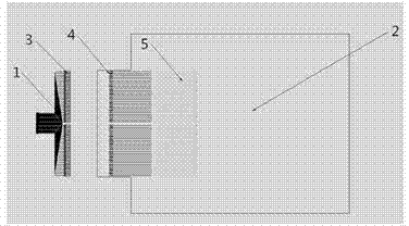
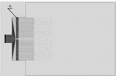
[0018] As shown in the figure, the present invention discloses a welding structure at the flick of the touch film, including: a touch film 2 and a flexible circuit board 1, and a number of fine wire sensors 5 are distributed on the flick of the touch film. ; The back side of the flexible circuit board is connected to an insulating pad, and the micro wire sensor is connected to the insulating pad. The fine wire sensor is soldered to the insulating pad by soldering. figure 1 It is a structural schematic diagram when the tail flick of the touch film of the present invention is separated from the flexible circuit board; figure 2 It is a schematic diagram of the structure when the tail flick of the touch film of the present invention is connected to the flexible circuit board; w...


PUM


Abstract

The invention discloses a welding structure at a tail of a touch control film. The welding structure comprises a touch control film and a flexible circuit board, wherein a plurality of fine wire sensors are distributed on the tail of the touch control film; an insulation welding disc is connected with the back surface of the flexible circuit board; and the fine wire sensors are connected to the insulation welding disc. The welding structure effectively avoids deformation of the touch control film due to high temperature during tin soldering; in addition, the flexible circuit board is directly adhered to the tail part of the touch control film; no objects are required to be adhered; production procedures are decreased; the production efficiency is improved; for the touch control film with the long side tail, the size of a packaging barrel of the touch control film is also greatly reduced; the cost of packaging materials and transportation cost are lowered; and the production cost is saved.

Description

technical field [0001] The invention relates to the field of electronics, in particular to a welding structure at the tail flick of a touch film. Background technique [0002] Projected capacitive touch film is a kind of sensing film mainly packaged with fine wires. It integrates the advantages of precise sensing positioning, flexibility and high transparency. It is used for precise touch positioning of touch screens above 12 inches, and is also used in precise Interactive projection. [0003] Projected capacitive technology is a kind of horizontal and vertical electrode arrays made on the surface of glass or transparent film. These horizontal and vertical electrode capacitance changes are used to detect finger touches. According to the difference in capacitance generation, it is divided into two types: Types of: [0004] Self-capacitance touch film is made of transparent conductive material on the surface of glass or transparent film to form horizontal and vertical electr...

Claims


Application Information

Patent Timeline
Patent Type & Authority Applications(China)
IPC IPC(8): G06F3/044
CPCG06F3/044
Inventor 罗延廷
Owner 罗延廷
Why Eureka
Try Eureka