Colloid removing method of quad flat no-lead packaging chip

A leadless packaging, square and flat technology, applied in the direction of electrical components, semiconductor/solid-state device manufacturing, circuits, etc., can solve the problem of difficult removal of residual glue 31

Active Publication Date: 2015-04-15
蔡宜兴
View PDF6 Cites 9 Cited by
  • Summary
  • Abstract
  • Description
  • Claims
  • Application Information

AI Technical Summary

Problems solved by technology

[0006] In summary, there is an urgent need to provide a further improved method for removing glue from QFN packaged chips, so as to improve the disadvantage that the glue 3 is di...

Method used


Image

  • Colloid removing method of quad flat no-lead packaging chip
  • Colloid removing method of quad flat no-lead packaging chip
  • Colloid removing method of quad flat no-lead packaging chip

Examples


Embodiment Construction

[0035] In order to make the above and other purposes, features and advantages of the present invention more comprehensible, the preferred embodiments of the present invention are specifically cited below, together with the accompanying drawings, as follows:

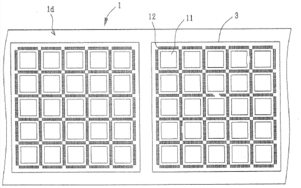
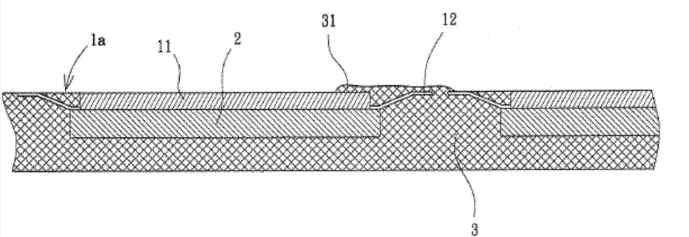
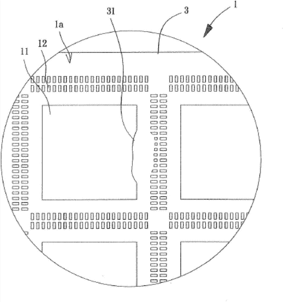
[0036] Please refer to Figure 4 Shown is a flow chart of a method for removing glue from a square flat no-lead package chip according to a preferred embodiment of the present invention. First, if Figure 5 and 6As shown, an image of a region R on the surface 1a of the substrate 1 is captured by a photomicrograph C. The photomicrograph C can be a Charge Coupled Device (CCD) camera or a complementary metal oxide Complementary Metal-Oxide Semiconductor (CMOS) camera, etc., and then use a computing unit to load the image of the region R, and perform image analysis operations to identify each heat sink 11 in the region R, and locate all heat sinks in the substrate 1 Packaged Die 2 Position. Please also refer to Figure 7...


PUM


Abstract

A colloid removing method of a quad flat no-lead packaging chip is used for solving the existing problem of poor yield of quad flat no-lead packaging chips. The colloid removing method of the quad flat no-lead packaging chip includes: an image of a substrate is obtained by photographing through a photomicrography device, a plurality of chips are packaged in the substrate, the chips are electrically connected with a plurality of lead frames, the lead frames are formed on a surface of the substrate, and colloids are arranged among lead frames; the image of the substrate is loaded by use of an arithmetic unit, based on which image analysis operation is executed to locate the chips packaged in the substrate; and the arithmetic unit compares each chip with a sample image, so as to detect the part of the lead frame electrically connected with each chip which is covered by residual gum of the colloid and is judged to be a redundant block of the colloid that needs ablation, a laser trajectory of a laser generator is set according to the redundant block, and the laser generator ablates and removes the redundant block of the colloid.

Description

technical field [0001] The invention relates to a deglue method for a square flat non-lead packaging chip, in particular to a deglue method for a square flat non-lead package chip that utilizes laser beam ablation to remove glue. Background technique [0002] Please refer to figure 1 and 2 Shown is a substrate 1 (substrate) used in a known quad flat no-lead package (QFN package) process, and a plurality of chips 2 (die) are packaged in the substrate 1 . The substrate 1 includes a plurality of heat sinks 11 (thermal pads), and corresponding to each of the heat sinks 11, a plurality of lead frames 12 (lead frames) are respectively provided, and the heat sink 11 and the plurality of lead frames 12 are formed on the substrate 1 A surface 1a of. Each of the chips 2 can be respectively bonded to the plurality of heat sinks 11 , and electrically connected to the plurality of lead frames 12 corresponding to each of the heat sinks 11 . Wherein, there is a colloid 3 (mold cap) bet...

Claims


Application Information

Patent Timeline
IPC IPC(8): H01L21/02
CPCH01L21/02098H01L21/02082
Inventor 蔡宜兴
Owner 蔡宜兴
Why Eureka
Try Eureka