A bonding fixture

A bonding and fixture technology, which is applied in the direction of manufacturing tools, auxiliary devices, electrical components, etc., can solve the problems of high equipment modification cost, small output, high production cost, etc., and achieve the effect of easy operation, firm fixation, and simple structure

Active Publication Date: 2017-11-14
WUXI CHINA RESOURCE MICRO ASSEMBLY TECH
View PDF7 Cites 0 Cited by
  • Summary
  • Abstract
  • Description
  • Claims
  • Application Information

AI Technical Summary

Problems solved by technology

For the particularity of high-power IGBT module production, that is, single operation and small output, high production cost
The current technology is to increase the loading and unloading mechanism and the transformation of the guide rail, but the cost of equipment transformation is relatively high, which makes the production cost relatively high

Method used


Image

  • A bonding fixture
  • A bonding fixture
  • A bonding fixture

Examples


Embodiment Construction

[0029] In order to make the above objects, features and advantages of the present invention more comprehensible, the present invention will be further described in detail below in conjunction with the accompanying drawings and specific embodiments.

[0030] Reference herein to "one embodiment" or "an embodiment" refers to a particular feature, structure or characteristic that can be included in at least one implementation of the present invention. "In one embodiment" appearing in different places in this specification does not all refer to the same embodiment, nor is it a separate or selective embodiment that is mutually exclusive with other embodiments.

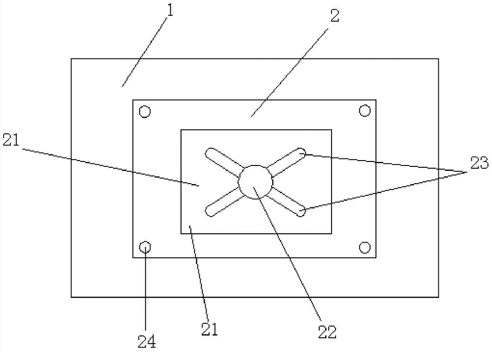
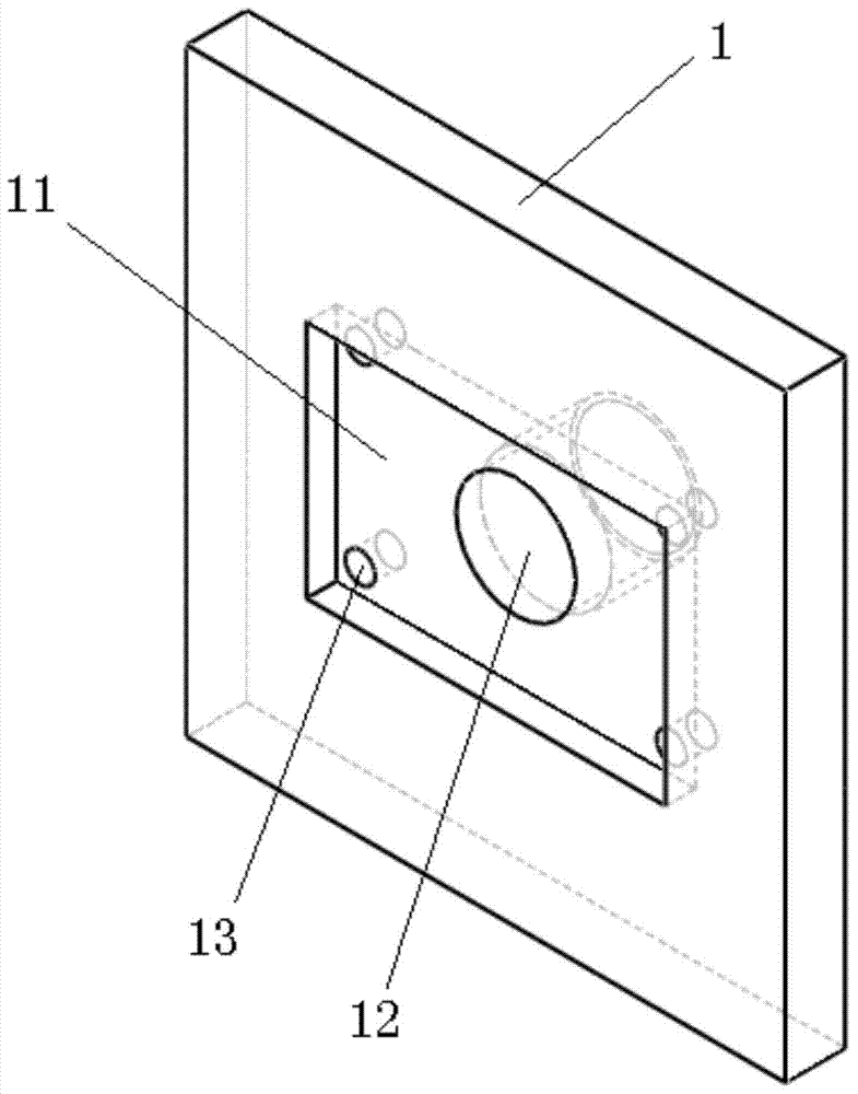
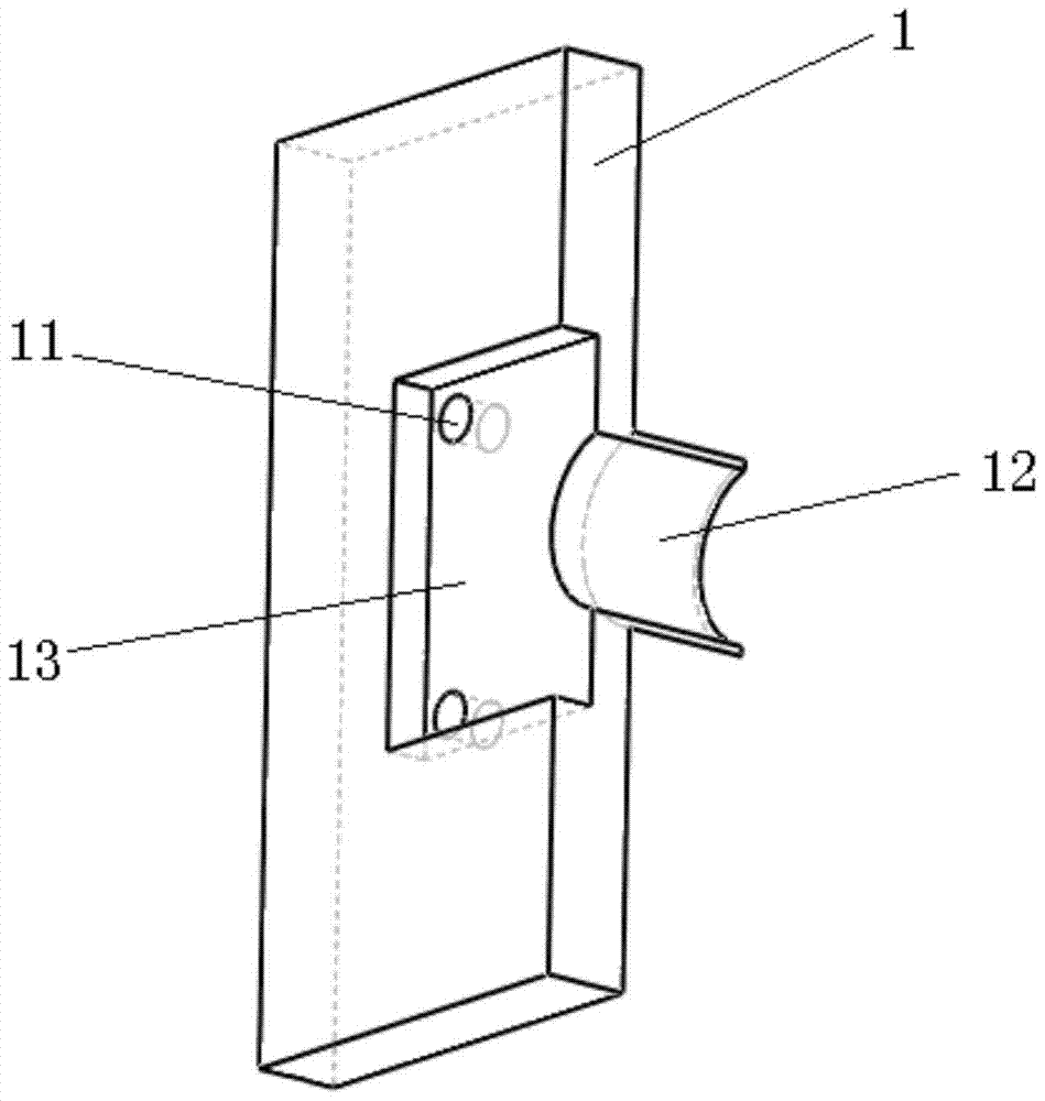
[0031] see figure 1 , which is a schematic diagram of the assembly of the vacuum base and the bonding limit fixture in the present invention. Such as figure 1 The bonding fixture includes a vacuum base 1 and a bonding limit fixture 2 . The vacuum base 1 is provided with a first accommodating cavity for accommodating the b...


PUM


Abstract

The invention provides a bonding clamp. The bonding clamp comprises a vacuum base and a bonding and limiting clamp, wherein the vacuum base is provided with a first accommodation cavity and a connecting hole communicated with the first accommodation cavity, the bonding and limiting clamp is accommodated in the first accommodation cavity, the bonding and limiting clamp is provided with a second accommodation cavity used for accommodating a DBC (direct bonding copper) substrate, the second accommodation cavity is provided with a second through hole communicated with the connecting hole; negative pressure is formed in the connecting hole and the second through hole to be attracted to the DBC substrate, and the DBC substrate is fixed in the second accommodation cavity. Compared with the prior art, the bonding clamp is simple in structure and easy to operate, and is simple to convert for different products, thus, debugging time for product conversion is greatly shortened. In addition, the DBC substrate is sucked through vacuum, so that the DBC substrate is firmly fixed, and on the premise of not affecting productivity, production cost is greatly reduced.

Description

technical field [0001] The present invention relates to the technical field of semiconductor module packaging, in particular to a bonding fixture used for packaging a direct bonding copper (Direct Bonding Copper, DBC) substrate of a semiconductor module. Background technique [0002] IGBT (Insulated Gate Bipolar Transistor, insulated gate bipolar transistor) module is a common intelligent power device, which is formed by packaging multiple IGBT chips (die) and other devices (such as power diodes) in combination (for example, in parallel with each other) . The DBC substrate is widely used in the packaging of IGBT modules, and it has the advantages of low cost, good heat dissipation, and good high-frequency performance. [0003] High-power IGBT modules need to be bonded with aluminum wires on the mounted DBC substrate. In order to ensure the quality of the bonding, the DBC substrate should not have a large vibration during the bonding process. Therefore, in order to ensure t...

Claims


Application Information

Patent Timeline
Patent Type & Authority Patents(China)
IPC IPC(8): H01L21/687H01L21/60B23K3/08
CPCH01L24/83H01L2224/8112H01L2224/818
Inventor 刘晓明龚平魏元华杨文波
Owner WUXI CHINA RESOURCE MICRO ASSEMBLY TECH
Why Eureka
Try Eureka