Semiconductor structure and formation method thereof

A semiconductor and interconnection structure technology, applied in the field of semiconductor structure and its formation, can solve the problems of volume increase and chip thickness increase, and achieve the effects of volume reduction, production cost reduction and high integration

Inactive Publication Date: 2015-04-15
SEMICON MFG INT (SHANGHAI) CORP
View PDF4 Cites 5 Cited by
  • Summary
  • Abstract
  • Description
  • Claims
  • Application Information

AI Technical Summary

Problems solved by technology

Although this packaging method stacks the chips together, it still increases the thickness of the chip, which increases the volume occupied by the entire packaging structure.

Method used


Image

  • Semiconductor structure and formation method thereof
  • Semiconductor structure and formation method thereof
  • Semiconductor structure and formation method thereof

Examples


Embodiment Construction

[0031] As mentioned in the background technology, the existing integrated passive devices are integrated on the first substrate, the corresponding CMOS devices are integrated on the second substrate, and then the first substrate and the second substrate are packaged together, but this packaging structure occupies The size is still very large.

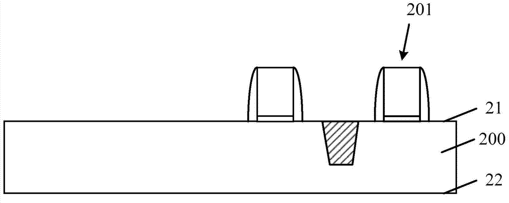
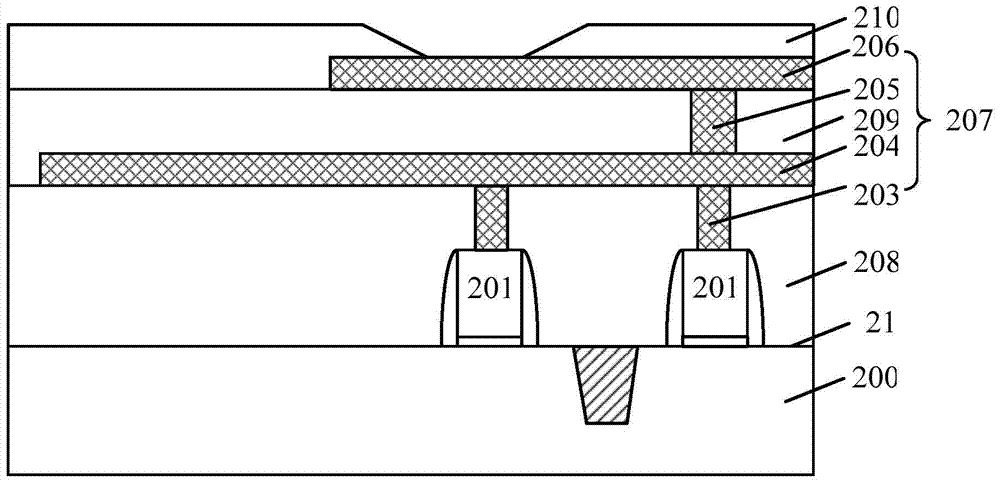
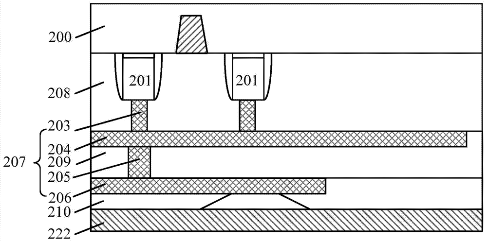
[0032] The present invention proposes a semiconductor structure and its manufacturing method. A CMOS device is formed on the first surface of the semiconductor substrate, and then a passive device is formed on the second surface of the semiconductor substrate. By penetrating the semiconductor substrate and part of the first medium The second metal interconnection layer of the second layer connects the passive device and the CMOS device together, while ensuring the integration of the device, it reduces the volume occupied by the entire semiconductor structure and reduces the manufacturing cost.

[0033] In order to make the above objects...


PUM


Abstract

Disclosed are a semiconductor structure and a formation method thereof. The semiconductor structure comprises a semiconductor substrate, a plurality of CMOS (complementary metal oxide semiconductor) devices, a first medium layer, a first interconnection structure, a through hole, an isolation layer, a second metal interconnection layer, a second medium layer and a plurality of passive devices. The semiconductor substrate comprises a first surface and a second surface, the CMOS devices are arranged on the first surface, the first medium layer covers the first surface and the CMOS device, the first interconnection structure is arranged in the first medium layer and connected with the CMOS devices, the through hole penetrates through the second surface of the semiconductor substrate and a part of the first medium layer, and the surface of the bottom of the first interconnection structure is exposed at the bottom of the through hole; the isolation layer is arranged on the side wall of the through hole and the second surface; the second metal interconnection layer is arranged on the isolation layer and at the bottom of the through hole and is connected with the surface of the bottom of the first interconnection structure; the second medium layer covers the second metal interconnection layer, and the through hole is filled with the second medium layer; the passive devices are arranged on the second medium layer, and one end of each passive device is connected with the second metal interconnection layer. The semiconductor structure is small in occupation space and high in integrity.

Description

technical field [0001] The invention relates to the field of semiconductor manufacturing, in particular to a semiconductor structure and a forming method thereof. Background technique [0002] With the development of electronic technology, the integration of active electronic components has been greatly improved after the semiconductor has entered the nanometer process from the micron process, and the demand for passive components that match active components has increased significantly. The market development trend of electronic products is light, thin, and small. Therefore, the improvement of semiconductor manufacturing capabilities has greatly increased the number of active components in the same volume. In addition to the substantial increase in the number of supporting passive components, more space is also required to place these passive components. Components, therefore, will inevitably increase the volume size of the overall packaged device, which is very different f...

Claims


Application Information

Patent Timeline
Patent Type & Authority Applications(China)
IPC IPC(8): H01L27/04H01L21/768H01L21/77
Inventor 李新戚德奎
Owner SEMICON MFG INT (SHANGHAI) CORP
Why Eureka
Try Eureka