Fan-out wafer level chip packaging method

A chip packaging, wafer-level technology, applied in the direction of electrical components, electrical solid devices, semiconductor/solid device manufacturing, etc., can solve the problems of low I/O terminal density, single structure, high cost, etc., to achieve wide application and multiple structures The effect of changing and enhancing the support strength

Active Publication Date: 2015-04-22
NANTONG FUJITSU MICROELECTRONICS
View PDF6 Cites 4 Cited by
  • Summary
  • Abstract
  • Description
  • Claims
  • Application Information

AI Technical Summary

Problems solved by technology

[0009] In order to overcome the problems of high cost, relatively low I / O terminal density, low strength and single structure in fan-out wafer-level chip packaging in the prior art, the present invention provides a fan-out wafer-level chip packaging The method comprises the steps of: encapsulating the chip 8, the wire 9, the conductive substrate 2 and the carrier 1 with a filler to form a plastic sealing layer 4; removing the carrier 1; filling the bottom of the plastic sealing layer 4 and the conductive substrate 2 with a dielectric Layer 5

Method used


Image

  • Fan-out wafer level chip packaging method
  • Fan-out wafer level chip packaging method
  • Fan-out wafer level chip packaging method

Examples


no. 1 Embodiment approach

[0033] The first specific embodiment: a fan-out wafer-level chip packaging method includes the following steps:

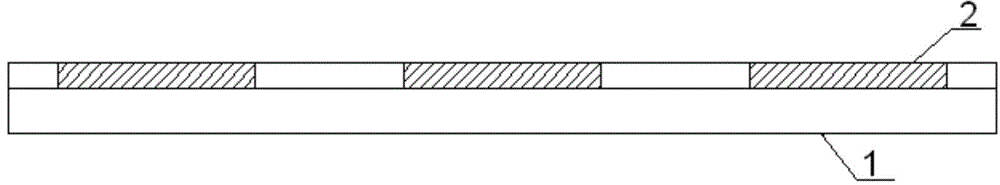
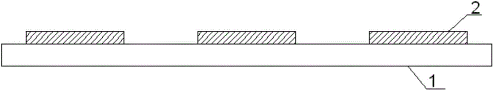
[0034] Such as figure 1 As shown, a carrier plate 1 is prepared, and the carrier plate 1 is made of a glass sheet or a silicon sheet or a ceramic sheet.

[0035] A conductive base material and a sticking film are formed on the carrier board 1 . A conductive substrate 2 is formed on the carrier 1 . Such as figure 2 as shown, figure 22 in is the conductive substrate 2, where the conductive substrate 2 is preferably a metal coating. Metal plating can be made on the carrier 1 by means of electroplating, electroless plating or sputtering. A film is pasted on the metal coating side of the carrier plate 1 so that the film material is distributed in a certain shape, and part of the metal coating is removed through exposure and development.

[0036] In another optional solution, the step of forming the conductive substrate 2 and the step of affixing a film on the ca...


PUM


Abstract

The invention provides a fan-out wafer level chip packaging method being characterized by comprising the following steps of packing a chip (8), wires (9), conductive substrates (2) and a support board (1) to form a plastic packaging layer (4) with filler, removing the support board (1), and filling the bottoms of the plastic packaging layer (4) and the conductive substrates (2) with conducting layers (6). The filler in the plastic packaging layer (4) is one or more of phenolic resin and reinforced unsaturated polyester resin. The fan-out wafer level chip packaging method achieves low cost and high precision through removing the support board (1) and wiring again at the bottom layer, and can be applied to various encapsulation modes, meanwhile, the distance between mounted balls can be reduced obviously through the composition of copper in a wire layer , and the entire supporting strength is reinforced.

Description

technical field [0001] The invention relates to the technical field of integrated circuit packaging, in particular to a fan-out wafer-level chip packaging method. Background technique [0002] In the current semiconductor industry, electronic packaging has become an important aspect of industry development. The development of packaging technology for decades has made high-density, small-size packaging requirements become the mainstream direction of packaging. Fan-out WLP is an embedded package processed at the wafer level, and it is also a major advanced packaging process with a large number of I / Os and high integration flexibility. Moreover, it enables vertical and horizontal multi-chip integration in one package without a substrate. As such, fan-out WLP technology is currently being developed into next-generation packaging technologies such as multi-die, low-profile packaging, and 3DSip. With the development of electronic products to be thinner, lighter, higher pin dens...

Claims


Application Information

Patent Timeline
Patent Type & Authority Applications(China)
IPC IPC(8): H01L21/56H01L21/60
CPCH01L21/568H01L24/02H01L24/80H01L24/81H01L2224/02379H01L2224/81H01L21/4846H01L21/56H01L21/6835H01L22/12H01L22/20H01L23/3128H01L23/49816H01L23/49861H01L24/29H01L24/32H01L24/45H01L24/48H01L24/49H01L24/83H01L24/97H01L2221/68345H01L2224/16225H01L2224/2929H01L2224/32225H01L2224/45124H01L2224/45144H01L2224/48091H01L2224/48227H01L2224/73204H01L2224/73265H01L2224/83121H01L2924/00014H01L2924/0781H01L2924/15311H01L2924/181H01L2924/186H01L2924/00H01L2924/00012H01L2224/05599
Inventor 石磊
Owner NANTONG FUJITSU MICROELECTRONICS
Why Eureka
Try Eureka