Soi wafer and its manufacturing method

a technology of soi wafer and manufacturing method, which is applied in the field of soi wafer, can solve the problems of low and achieve the effects of improving reliability of lpd evaluation of the active layer, reducing the contamination level of metal impurities in the active layer, and increasing the strength of the supporting wafer

Inactive Publication Date: 2007-02-08
SUMCO CORP
View PDF4 Cites 29 Cited by
  • Summary
  • Abstract
  • Description
  • Claims
  • Application Information

AI Technical Summary

Benefits of technology

[0066] According to the present invention, the supporting wafer contains the boron by an amount of 9×10¹⁸ atoms / cm3 or more. Owing to this, the metal impurities of Fe, Cu that has diffused outward and resultantly permeated through the buried insulating film among the metal impurities contained in the active layer wafer or the active layer as well as the metal impurities contained in the supporting wafer can be captured by the boron serving as the gettering site. As a result, the level of contamination from the metal impurities in the active layer can be reduced.
[0067] Further, since the boron is present in the crystal of ingot at a high concentration, the strength of the supporting wafer can be increased and thus the occurrence of the slip of the supporting wafer during the heat treatment can be prevented.
[0068] In addition, since no crystal defect exists in the supporting wafer, even if the film thickness is reduced in the active layer and the silicon oxide film, the LPD evaluation would not detect any micro voids present between the buried insulating film and the supporting wafer as the pseudo defects and so the reliability of the LPD evaluation of the active layer can be improved.
[0069] More advantageously, since such a bonded wafer as described above can be obtained simply by adding the boron by an amount of 9×10¹⁸ atoms / cm3 or more into the crystal at the time of pulling up of the ingot to be processed into the supporting wafer, the bonded wafer having the effects as described above can be manufactured favorably at a lower cost.
[0070] Further, since the oxide film has been formed at least on the surface opposite to the bonding surface of the supporting wafer before the step of bonding, this oxide film can help inhibit the boron from diffusing outward from the back surface of the supporting wafer during the heat treatment after the step of bonding. Consequently, the autodoping resultant from the boron attempting to intrude into the surface of the active layer wafer or the surface of the active layer can be prevented.
[0071] Still further, since the supporting wafer is subjected to the annealing at the temperature of 1100° C. or higher in the reducing gas atmosphere containing the hydrogen gas before the step of bonding, the boron present in the vicinity of the top and the back surfaces of the supporting wafer can disappear with the aid of the outward diffusion thereof. As a result, the autodoping of the boron into the surface of the active layer wafer or the surface of the active layer during the heat treatment after the step of bonding can be prevented, as well.

Problems solved by technology

As a result, the reliability of the LPD evaluation has been made low.

Method used


Image

  • Soi wafer and its manufacturing method
  • Soi wafer and its manufacturing method
  • Soi wafer and its manufacturing method

Examples


first embodiment

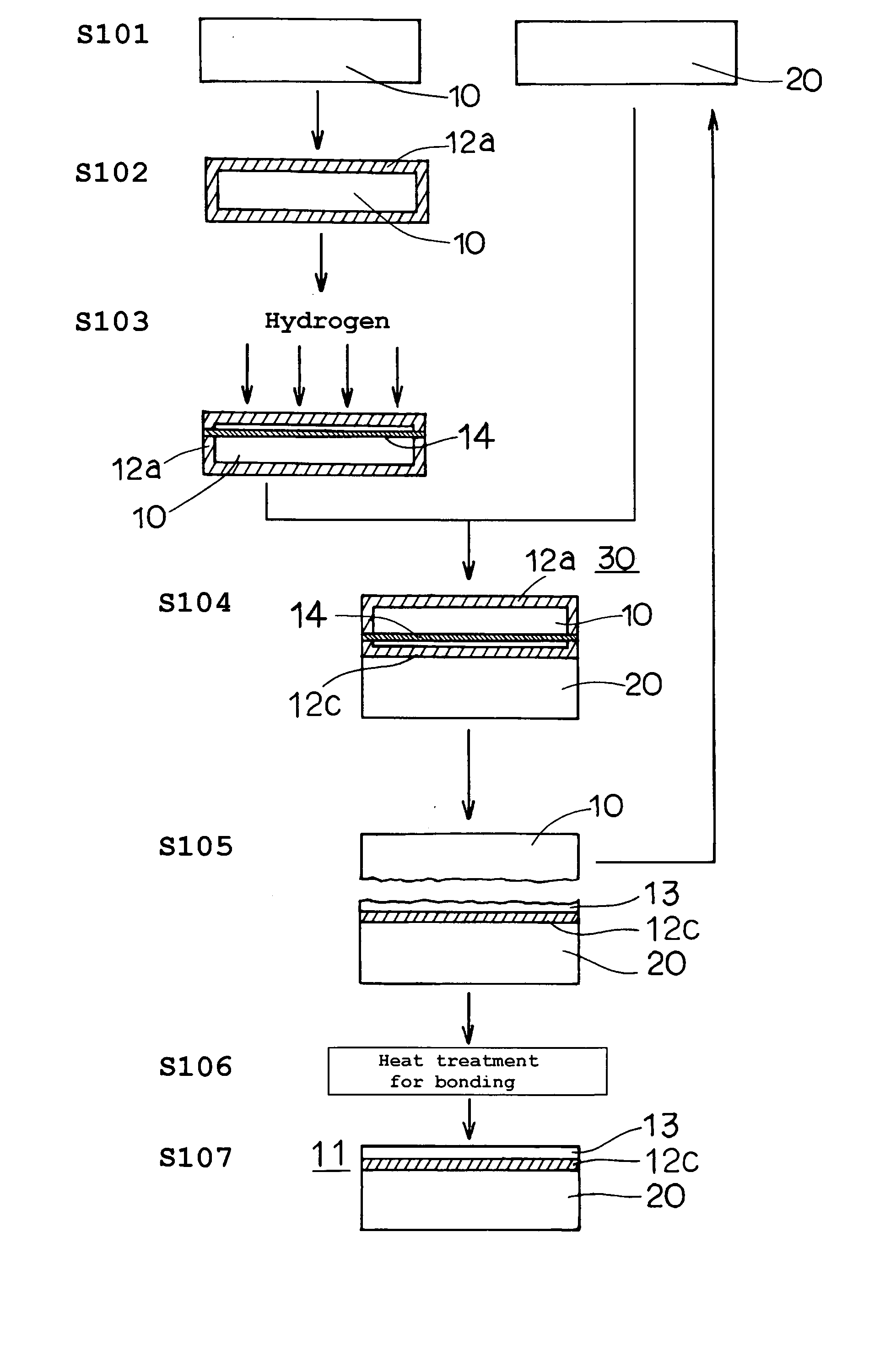
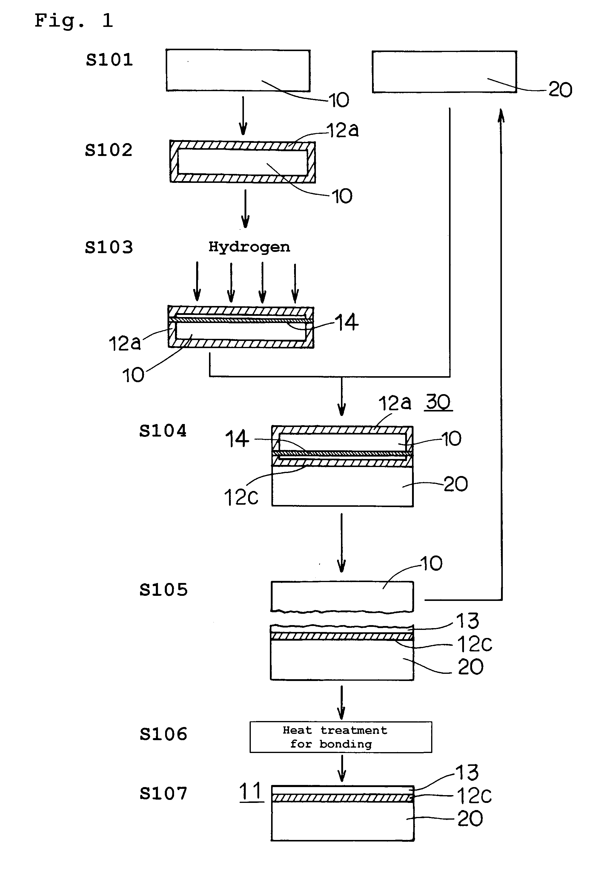
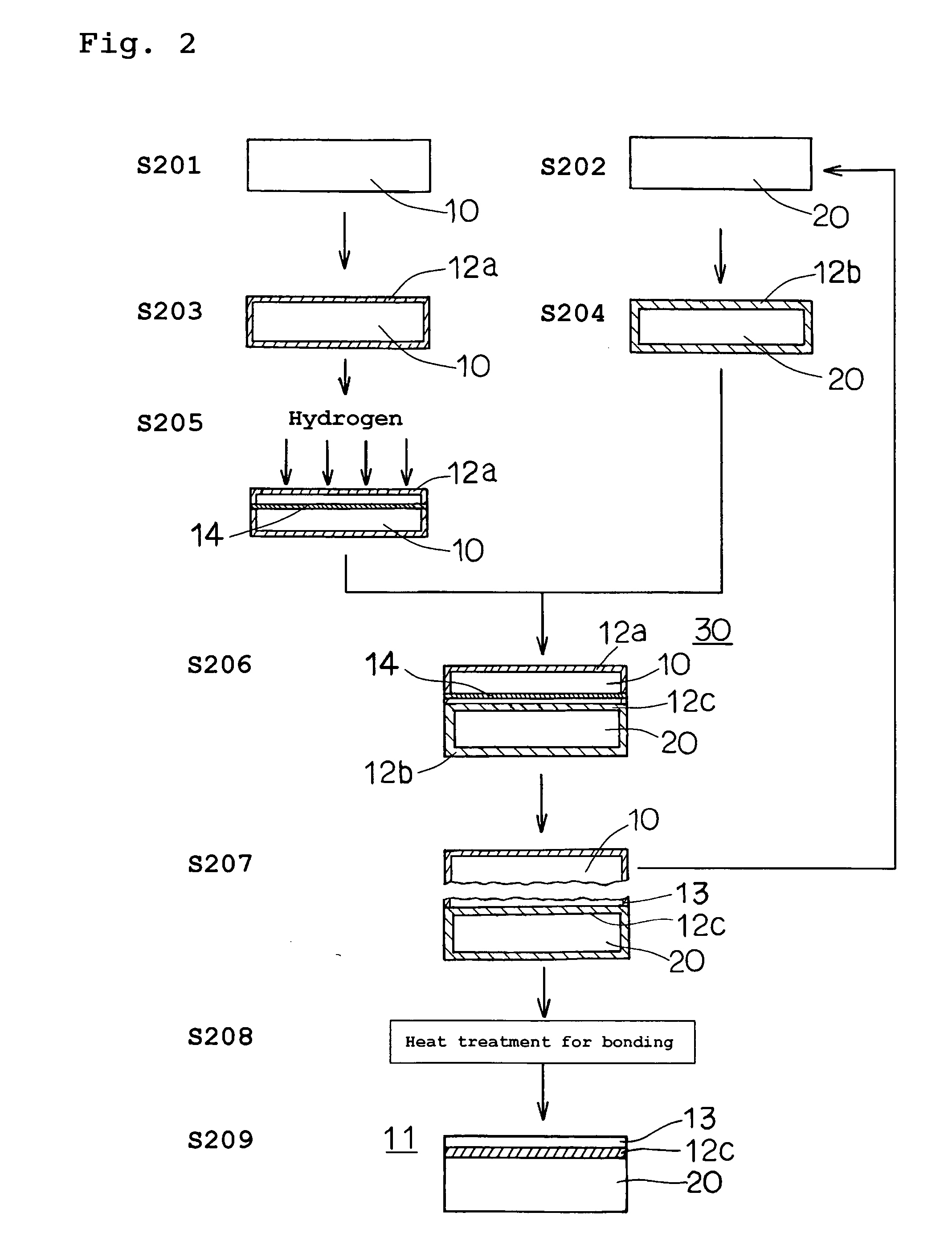
[0083] Firstly, a monocrystal ingot of silicon of p-type that has been added with boron at a low concentration by an amount of 2×10¹⁵ atoms / cm3 is pulled up in the CZ method, as shown in step 101 of FIG. 1. A rate of pulling up is 1.0 mm / min. After that, the monocrystal ingot of silicon undergoes a series of processing comprising block cutting, slicing, beveling and mirror polishing. Those steps of processing produce a wafer to be prepared as an active layer wafer 10 of p-type and mirror-polished having a thickness of 725 μm, a diameter of 200 mm, a face orientation of (100) face, a specific resistance of 10 Ωcm.

[0084] On the other hand, a monocrystal ingot of silicon of p-type that has been added with the boron at a high concentration by an amount of 1×10¹⁹ atoms / cm3 is pulled up in the Cz method. After that,the monocrystal ingot of silicon undergoes a series of processing comprising block cutting, slicing, beveling and mirror polishing. Those steps of processing produce a wafer t...


PUM

PropertyMeasurementUnit
thicknessaaaaaaaaaa
temperatureaaaaaaaaaa
thicknessaaaaaaaaaa

Abstract

Since a supporting wafer contains boron of 9×10¹⁸ atoms/cm3 or more, therefore a part of the metal impurities in an active layer wafer and the metal impurities in the wafer can be captured by the boron during the heat treatment for bonding. As a result, metal contamination in the active layer can be reduced. Moreover, the wafer strength is enhanced, thus preventing the wafer slipping. Since the wafer has no COP, micro voids are not detected in the LPD evaluation of the active layer, thereby improving the reliability of the evaluation. Such a bonded wafer can be manufactured at a low cast.

Description

FIELD OF THE INVENTION [0001] The present invention relates to an SOI wafer and a manufacturing method of the same, and more specifically to a technology for manufacturing an SOI wafer inexpensively by taking advantage of a bonding method capable of: decreasing a level of contamination resultant from metal impurities contained in an active layer; providing a sufficient strength to suppress an occurrence of slip of a supporting wafer; and improving precision in the LPD evaluation of the active layer of thin film. DESCRIPTION OF THE PRIOR ART [0002] Recently, film thickness reduction of an active layer (0.10 μm or thinner) has been progressed in conjunction with a highly densified integration of devices. There has been developed the smart cut method as a method for manufacturing a semiconductor substrate having an SOI (Silicon On Insulator) structure for achieving the above-mentioned film thickness reduction. [0003] In the smart cut method, firstly a wafer for active layer, which has ...

Claims


Application Information

Patent Timeline
Patent Type & Authority Applications(United States)
IPC IPC(8): H01L21/30H01L21/46H01L21/322H01L21/762H01L27/12
CPCH01L21/322H01L21/76254H01L21/3225
Inventor ENDO, AKIHIKOMORIMOTO, NOBUYUKI
Owner SUMCO CORP
Why Eureka
Try Eureka