Solid state sensor for metal ion detection and trapping in solution

a solid-state sensor and metal ion technology, applied in the direction of liquid/fluent solid measurement, test/measurement of semi-solid devices, liquid/fluent solid measurements, etc., can solve the problem of destroying the devices being processed, ineffective solution in carrying out the intended function, and contamination of metal ions in the solution. problem, to achieve the effect of reducing the contamination level in the solution

Active Publication Date: 2015-04-07
WAFERTECH
View PDF10 Cites 0 Cited by
  • Summary
  • Abstract
  • Description
  • Claims
  • Application Information

AI Technical Summary

Benefits of technology

[0011]According to yet another aspect, the device, apparatus and method of the invention can be used to trap metal ions, thereby removing metal ions from a solution and reducing contamination levels in the solution.

Problems solved by technology

The metal ion contamination in the solution contaminates and can destroy the devices being processed in the solution and metal ion contamination is also indicative of a processing problem.
In addition to the metal ion contamination causing shorting or particle contamination of the device being processed in the solution, the contamination may result in ineffectiveness of the solution in carrying out its intended function.
This degradation can cause other equipment problems such as electrical problems and further contamination issues.
If the metal ion contamination goes undetected, additional devices become contaminated as they undergo processing and the cause of the contamination may become exacerbated.
These techniques, however, are time dependent and also depend on the loading effect in the solution and human error.
Moreover, the results obtained using these techniques are not real-time, in-situ results.

Method used


Image

  • Solid state sensor for metal ion detection and trapping in solution
  • Solid state sensor for metal ion detection and trapping in solution
  • Solid state sensor for metal ion detection and trapping in solution

Examples


Embodiment Construction

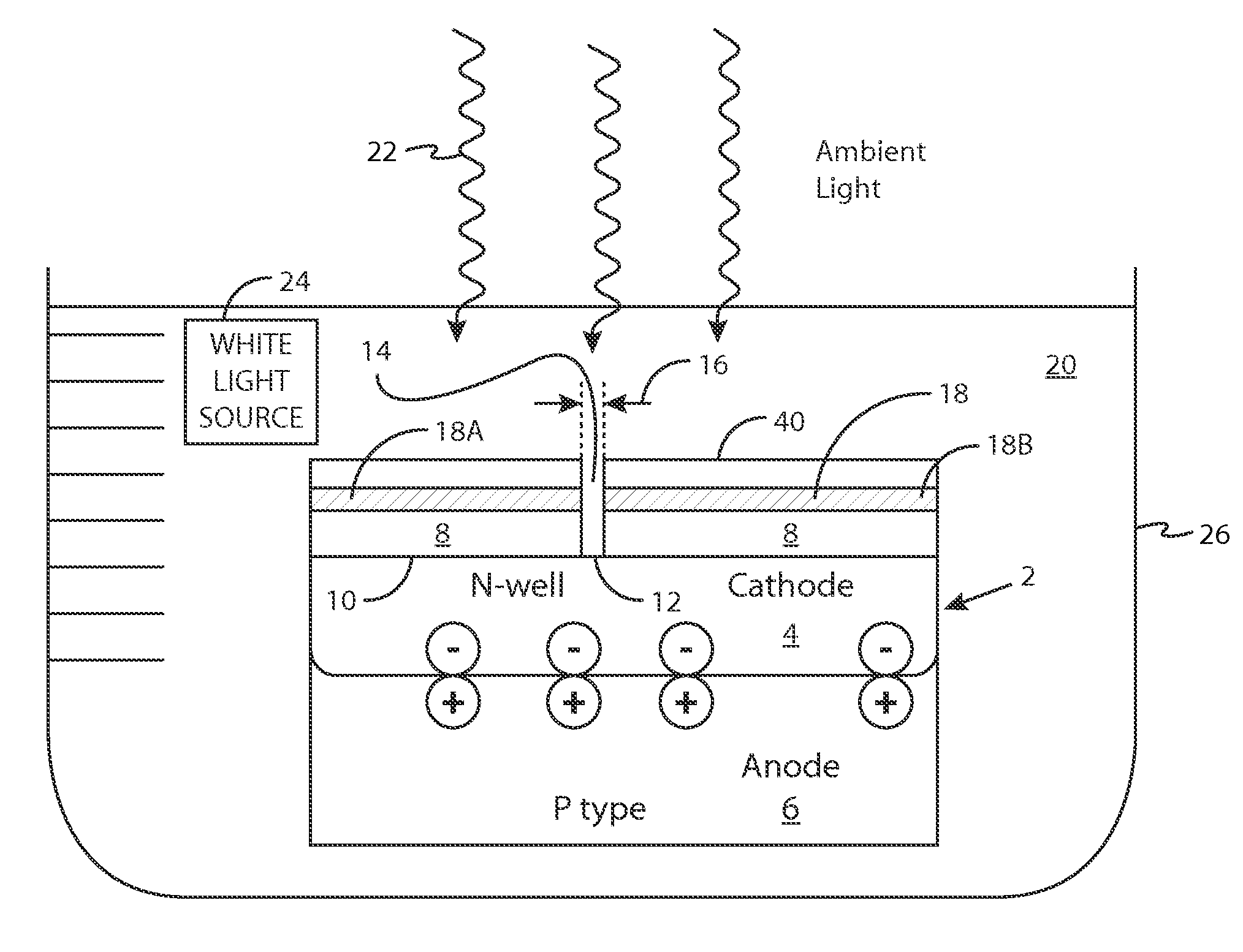
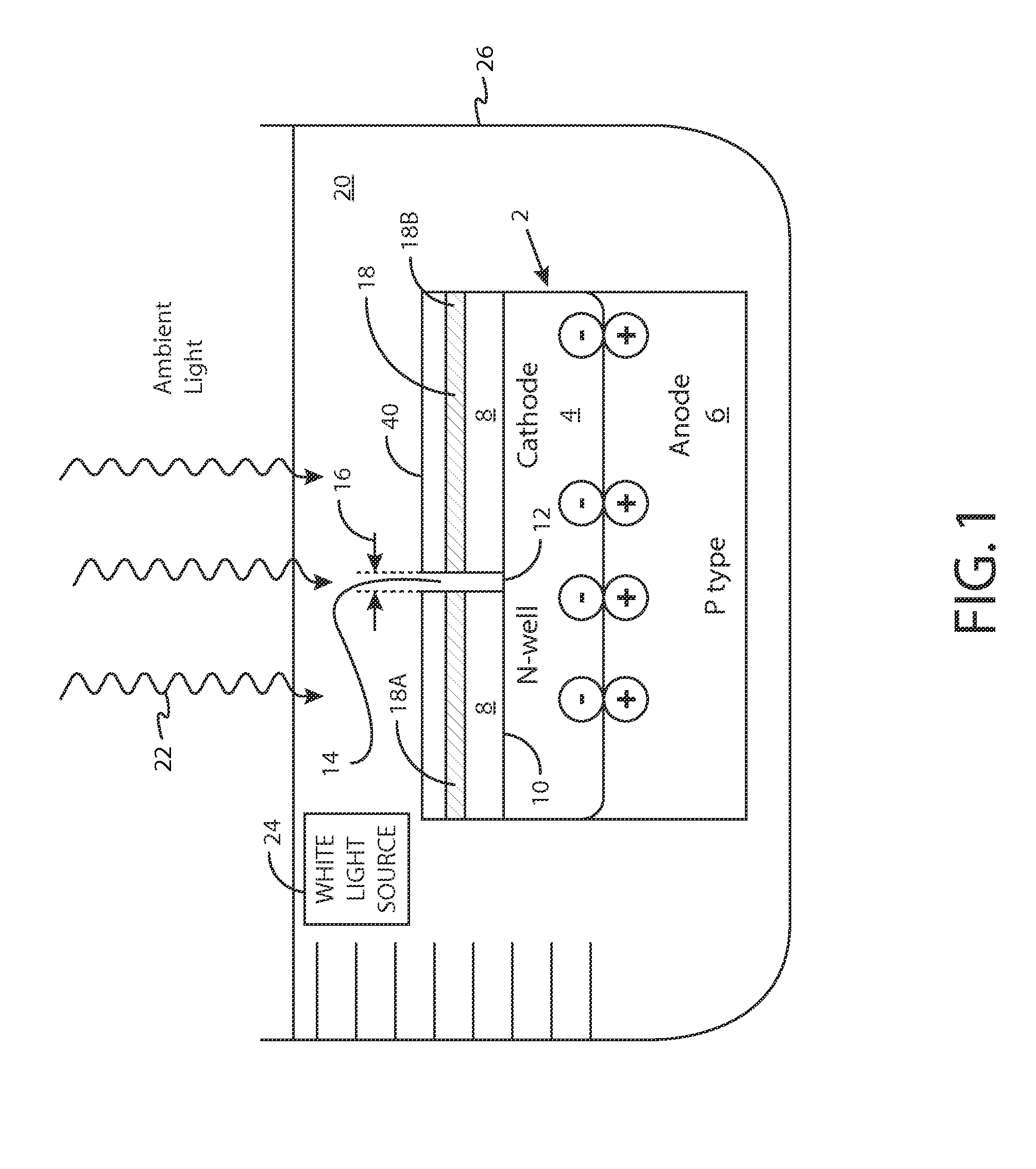
[0019]Provided is a metal ion detection device and method that can be used for in-situ detection of metal ion contamination in a solution and also for metal ion trapping, i.e. causing the metal ions to be drawn from the solution.

[0020]The metal ion detection device is a self-powered optical sensor array that is used for in-situ detection of metal ion contamination in solution. The detection device is sensitive enough to monitor metal ions before the concentration of metal ion contamination reaches a dangerous level, providing early warning and prevention of problems associated with metal ion contamination and pollution.

[0021]The metal ion detection device includes a semiconductor device with at least one area of N-type material, such as an N-well area, over a P-type material such as a P-type substrate and utilizes a photovoltaic operation to optically illuminate the semiconductor device creating a P / N junction with a voltage across the P / N junction.

[0022]The creation of the P / N junc...


PUM

PropertyMeasurementUnit
voltageaaaaaaaaaa
conductanceaaaaaaaaaa
concentrationaaaaaaaaaa

Abstract

A device, apparatus and method for trapping metal ions and detecting metal ion contamination in a solution provide a semiconductor device formed on a semiconductor substrate and including an N-well formed over a P-type substrate and at least a contact portion of the N-well in electrical contact with the solution. When the semiconductor device is optically illuminated, a P / N junction is formed as a result of photovoltaic phenomena. Metal ions from the solution migrate to the contact area due to the voltage created at the P / N junction. The semiconductor device includes a conductive structure with conductive features separated by a gap and therefore in an initially electrically open state. When the ions migrate to the contact area, they precipitate, at least partially bridging the gap and creating conductance through the conductive structure. The conductance may be measured to determine the amount of metal ion contamination.

Description

FIELD OF THE INVENTION[0001]The present invention relates to a device, apparatus and method for the analysis and detection of metal ions in a solution. The device, apparatus and method of the invention are further directed to the removal of metal ions from solution via metal ion trapping.BACKGROUND[0002]In today's advanced semiconductor manufacturing industry, it is of critical importance to prevent contamination in all processing operations and also to detect contamination and identify the type and source of contamination as soon as possible. This applies to wet chemistry processing operations as well as all other operations used to manufacture semiconductor devices such as dry chemical processing, chemical mechanical polishing (CMP), plasma processing operations, thin film deposition operations, photolithographic operations, wafer transport operations and the like.[0003]In wet chemical processing solutions or in other operations in which a chemical cleaning and / or rinsing solution...

Claims


Application Information

Patent Timeline
Patent Type & Authority Patents(United States)
IPC IPC(8): G01N27/07H01L21/66
CPCH01L22/10G01N27/07H01L2924/0002H01L2924/00G01N27/414
Inventor CHIU, RE-LONGHIGGINS, JASON
Owner WAFERTECH
Why Eureka
Try Eureka