Method for fabricating silicon targets

a technology of target silicon and silicon film, applied in the field of integrated circuit (ic) fabrication, can solve the problems of low attention to particle size and uniformity, the inability to form high-doped silicon film into a transistor active area, and the inability to achieve the effect of reducing the contamination level of deposited silicon film and excellent particle performan

Inactive Publication Date: 2005-04-12
SHARP LAB OF AMERICA INC
View PDF6 Cites 3 Cited by
  • Summary
  • Abstract
  • Description
  • Claims
  • Application Information

AI Technical Summary

Benefits of technology

The present invention involves a procedure to produce silicon targets for use in microelectronics, particularly in the fabrication of polycrystalline silicon TFTs. The silicon tiles and resultant targets demonstrate excellent particle performance and reduced contamination levels in the deposited silicon-films.
Accordingly, a method is provided for forming silicon target tiles in the fabrication of integrated circuit (IC) sputter deposited silicon films. The method comprises: cutting either single-crystal or polycrystalline silicon tiles to a thickness in the range of 7 millimeters (mm) to 10 mm; and, treating the silicon tile edges to minimize the generation of contaminating particles. The silicon tile treatment includes subjecting the silicon tile top and bottom surface edges to a beveling or radiusing operation. The silicon tile top surface edges are beveled within the range of 1 mm to 5 mm, or radiused within the range of 3 mm to 10 mm. The silicon tile bottom surface edges are beveled approximately 1.5 mm. Further, the silicon tile treatment includes beveling the silicon tile corners approximately 1.5 mm.

Problems solved by technology

However, a highly doped silicon film cannot be formed into a transistor active area.
Furthermore, these optical coatings are a continuous blanket films and, therefore, little regard is paid to particle size and uniformity.
Particles larger than approximately 5 microns are not desirable in TFT process films.
High particle levels result in low yields, as well as reduced equipment up-time, since frequent cleaning of the chamber is required.
The issue of particles is particularly severe for silicon targets for two reasons: (1) the target is a tiled assembly (not a single piece), which means that the edges of the tiles can generate particles, unless they are properly prepared; and, (2) the target material is generally of low resistivity (does not conduct thoroughly) as a result of the purity requirements of the deposited film.
Hence, the material is susceptible to charge buildup and, consequently, arcing, especially if the surface of the target is not properly conditioned.
Arcing may result in increased contamination in the film, especially with the material that the chamber and internal components being made of Al, Ni, or equivalent metals.

Method used


Image

  • Method for fabricating silicon targets
  • Method for fabricating silicon targets
  • Method for fabricating silicon targets

Examples


Embodiment Construction

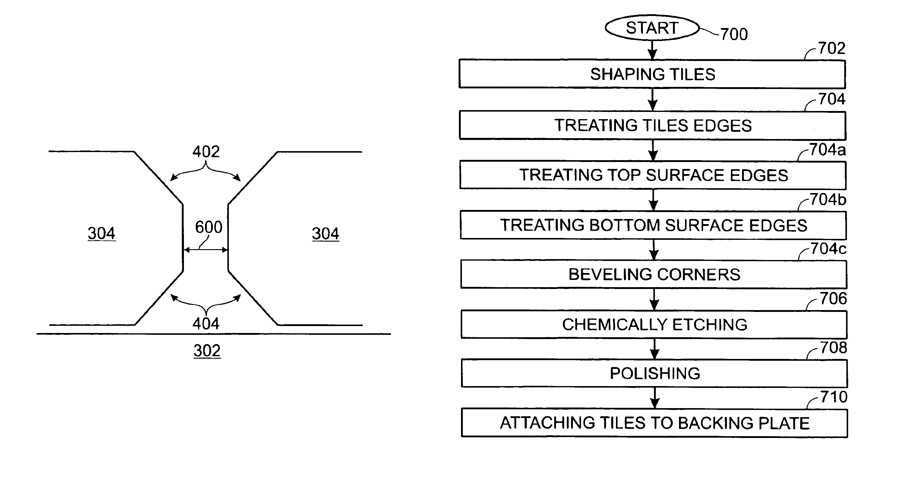
The present invention describes the fabrication of silicon targets using either single-crystal silicon material or using polysilicon material. The material of the target is important in determining the number of tiles in the final target. A silicon target with a surface of 650 millimeters (mm) by 550 mm requires about 20 single-crystal silicon (c-Si) tiles, but only 4 polysilicon (p-Si) tiles. The number of single-crystal tiles can be reduced by accepting an orientation of silicon material, other than the standard (100) crystallographic orientation. That is, the silicon tiles can be cut lengthwise from the silicon ingot. However, it is likely that a target made from single-crystal material will always include more tiles than a similarly-sized target made from polycrystalline silicon material. The number of tiles affects the overall area of tile edge as well as the number of tile gaps across the face of the target. For this reason, it is best to minimize the number of tile gaps in th...


PUM

PropertyMeasurementUnit
thicknessaaaaaaaaaa
flatnessaaaaaaaaaa
flatnessaaaaaaaaaa

Abstract

A method for fabricating silicon tiles and silicon tile targets has been provided, such as may be used in the sputter deposition of thin film transistor (TFT) silicon films. The method describes processes of cutting the tiles, beveling the tiles edges, etching the tiles to minimize residual damage caused by cutting the tiles, polishing the tiles to a specified flatness, and attaching the tiles to a backing plate. All these processes are performed with the aim of minimizing contamination and particle formations when the target is used for sputter deposition.

Description

BACKGROUND OF THE INVENTION1. Field of the InventionThis invention generally relates to integrated circuit (IC) fabrication and, more particularly, to a system and method for forming silicon targets for use in sputter deposition processes.2. Description of the Related ArtResearch continues into methods of producing polycrystalline (p-Si) film by annealing amorphous silicon (a-Si) films. Polycrystalline films are used in the formation of IC active areas, such as the source, drain, and gate regions of a transistor. One specific application is the formation of thin film transistors (TFTs) that are used in the fabrication of active matrix (AM) liquid crystal displays (LCDs).One relatively recent approach to forming an amorphous silicon film is through silicon (Si) sputter deposition. Little prior art exists in this field, as the application of sputtering method for silicon deposition in microelectronics (i.e. TFTs) is quite new. There is a body of work in the use of silicon targets for ...

Claims


Application Information

Patent Timeline
Patent Type & Authority Patents(United States)
IPC IPC(8): C23C14/56C23C14/34C30B33/00H01L29/66H01L21/02H01L21/336H01L29/786H01L21/203
CPCC23C14/3407C23C14/564C30B29/06H01L29/66757H01L29/78675C30B33/00Y10S438/977
Inventor VOUTSAS, APOSTOLOSHARTZELL, JOHN
Owner SHARP LAB OF AMERICA INC
Why Eureka
Try Eureka